
DBC substrate capable of reducing heat warping

A substrate and copper layer technology, applied in the direction of semiconductor/solid-state device components, semiconductor devices, electrical components, etc., can solve the problems of warping deformation, delamination of DBC substrates, reducing the reliability and life of power semiconductor devices, etc., to improve The effect of thermal cycle life

Pending Publication Date: 2022-07-15
HUAZHONG UNIV OF SCI & TECH
View PDF0 Cites 1 Cited by
  • Summary
  • Abstract
  • Description
  • Claims
  • Application Information

AI Technical Summary

Problems solved by technology

During the high temperature and low temperature cycle operation, the DBC substrate is thermally expanded, that is, due to the different thermal expansion coefficients of ceramics and copper, the interface between the copper layer and the ceramic layer is bent due to the mismatch of expansion dimensions, and the local stress concentration is different, resulting in delamination and fracture. , reducing the reliability and lifetime of power semiconductor devices
[0004] At present, in the existing technology, there is no corresponding technical solution to solve the problem of warping and deformation of the DBC substrate after being heated.

Method used


Image

  • DBC substrate capable of reducing heat warping
  • DBC substrate capable of reducing heat warping
  • DBC substrate capable of reducing heat warping

Examples


Embodiment Construction

[0033] In order to make the objectives, technical solutions and advantages of the present invention clearer, the present invention will be further described in detail below with reference to the accompanying drawings and embodiments. It should be understood that the specific embodiments described herein are only used to explain the present invention, but not to limit the present invention. In addition, the technical features involved in the various embodiments of the present invention described below can be combined with each other as long as they do not conflict with each other.

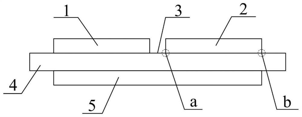
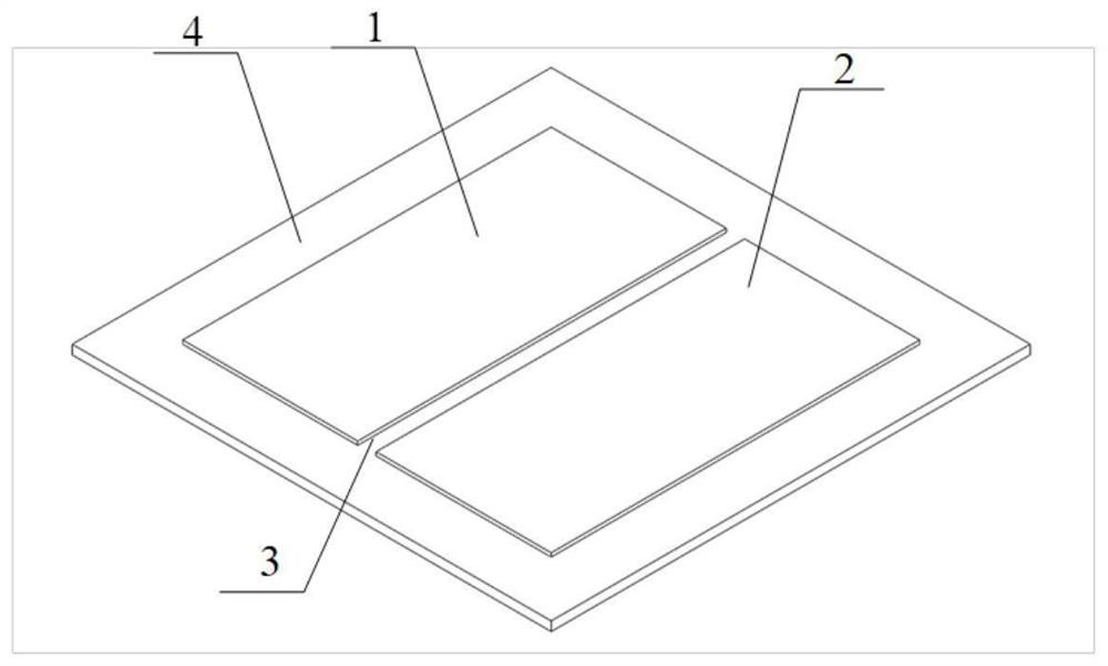
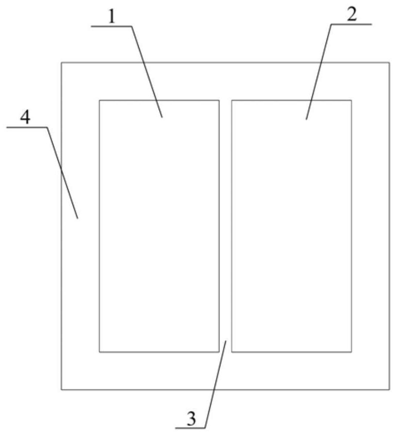
[0034] like figure 1 As shown, the DBC substrate structure provided by the present invention mainly includes, from top to bottom: a top copper layer 1, an insulating ceramic layer 4 and a bottom copper layer 5, and a plurality of components arranged side by side are opened on the top copper layer 1 The welding area is used for electrical isolation and circuit formation inside the power module; an i...


PUM

PropertyMeasurementUnit
widthaaaaaaaaaa
diameteraaaaaaaaaa
thicknessaaaaaaaaaa

Abstract

The invention discloses a DBC substrate capable of reducing heat warping, and belongs to the technical field of power semiconductors. The structure sequentially comprises a top copper layer, an insulating ceramic layer and a bottom copper layer from top to bottom, the top copper layer is provided with a plurality of component welding areas which are arranged in parallel, and an insulation gap is arranged between every two adjacent component welding areas; the bottom copper layer is provided with a load reducing groove area, the load reducing groove area coincides with the vertical center line of the insulation gap, and the width of the load reducing groove area is not smaller than the width of the insulation gap. A plurality of load reducing grooves distributed in an array shape are formed in the load reducing groove area. The bending degree of the bottom copper layer in the area is changed by arranging the load reducing grooves distributed in the array shape, and buckling deformation caused by different thermal expansion coefficients of materials of the insulating ceramic layer and the bottom copper layer when the DBC substrate is heated can be reduced; original concentrated stress can be weakened, and the thermal cycle life of the substrate is prolonged.

Description

technical field [0001] The invention belongs to the technical field of power semiconductors, and more particularly, relates to a DBC substrate with reduced thermal warpage. Background technique [0002] As the core power electronic devices, power semiconductor devices have been widely used in power systems, rail transit, industrial manufacturing equipment, household appliances, military defense and many other fields, and are constantly moving towards high power, miniaturization, integration and multi-functionality. Development has also put forward higher requirements for the performance of packaging substrates. With the increase of power density, the operating temperature of power modules increases significantly, and it is challenging to improve their reliability and fatigue life. [0003] Direct bonded copper (DBC for short) is a very important power electronic packaging material. It has excellent thermal conductivity, high adhesion strength between metal and ceramic, good...

Claims


Application Information

Patent Timeline
Patent Type & Authority Applications(China)
IPC IPC(8): H01L23/498H01L23/367H01L23/373
CPCH01L23/49838H01L23/49861H01L23/49811H01L23/3672H01L23/3731
Inventor 陈材张弛杜梦瑶康勇
Owner HUAZHONG UNIV OF SCI & TECH
Learn More