


Quick Research
Generate reliable direction feasibility study reports for your R&D in just a few steps.

Technical Q&A
Discover and master advanced knowledge NOW. Basics, ideas, possibilities, all at once.

Find Solutions
As an expert in R&D theories, this can generate solutions to your technical problems instantly.

Evaluate Feasibility
Analyze your overall solution with one click, know your potential R&D risks in advance.

Monitor Landscape
Get weekly tech updates, stay abreast of the latest tech innovations and key insights.
LED packaging device
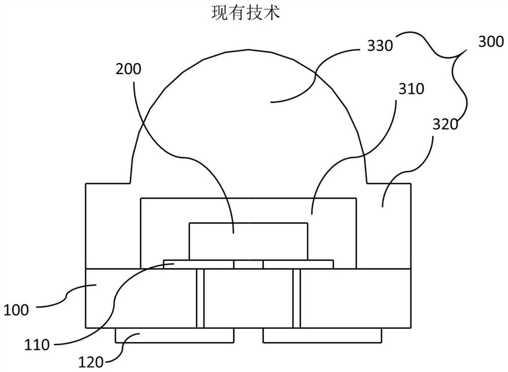
A technology of LED packaging and LED chips, which is applied in the direction of semiconductor devices, electrical components, circuits, etc., can solve the problems of increasing packaging costs, product scrapping, and easy breakage, and achieve the goal of reducing overall cost, reducing edge stress, and increasing light extraction rate Effect
- Summary
- Abstract
- Description
- Claims
- Application Information
AI Technical Summary
Problems solved by technology
Method used
Image

Examples
no. 1 example
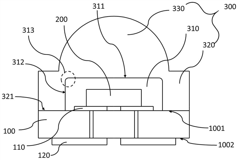
[0031] According to one aspect of the present application, an LED package device is provided. see figure 2 , figure 2 It is a cross-sectional view of the LED package device according to the first embodiment of the present application. The LED package device includes a package substrate 100 , an LED chip 200 and a light-transmitting unit 300 . The package substrate 100 has a first surface 1001 and a second surface 1002 disposed opposite to each other. The LED chip 200 is disposed on the first surface 1001 of the package substrate 100 . The light-transmitting unit 300 is disposed on the first surface 1001 of the package substrate 100 , and has an inner cavity 310 , and the LED chip 200 is located in the inner cavity 310 . The inner cavity 310 has an upper surface 311 and a side surface 312, the upper surface 311 and the side surface 312 have a first connecting portion 313, and the first connecting portion 313 is a curved surface or an inclined surface or a combination ther...
no. 2 example
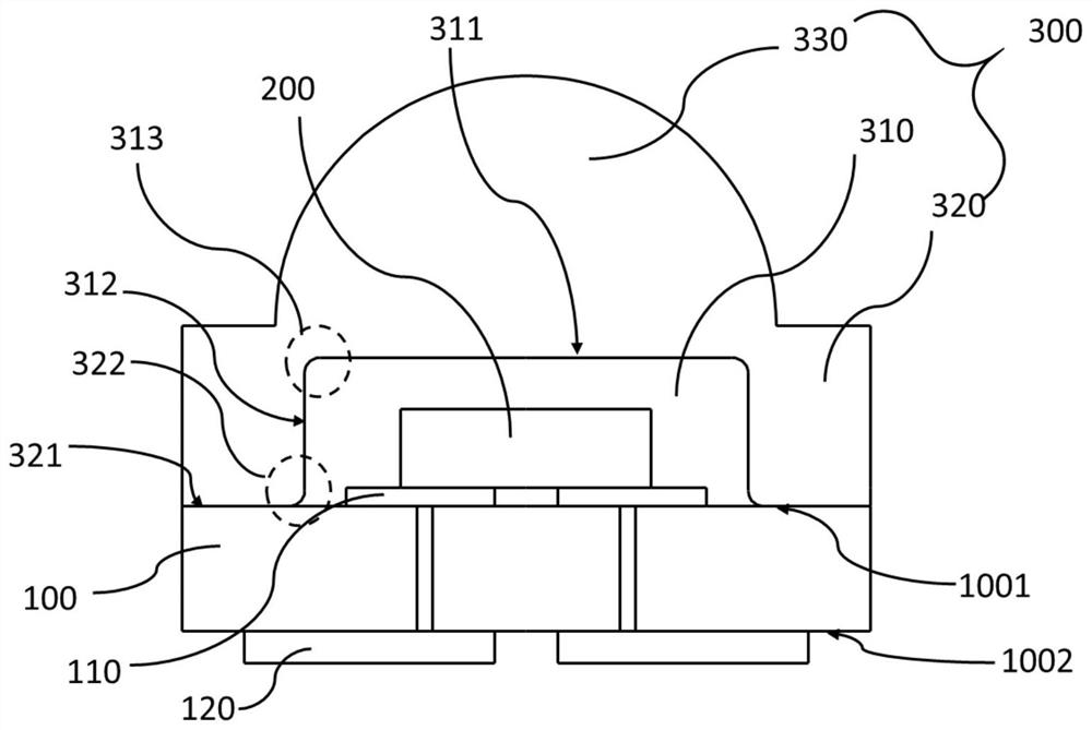
[0040] image 3 It is a schematic cross-sectional view for explaining the LED package device of the second embodiment of the present application. The difference from the first embodiment is:
[0041] The light-transmitting unit 300 includes a base 320 and a light-transmitting area 330 . The base 320 has a lower surface 321 in contact with the first surface 1001 of the package substrate. The second connecting portion 322 is a curved surface, and the curved surface has a changing slope. In a specific embodiment, the second connecting portion 322 is a rounded corner, that is, an arc-shaped edge is formed between the lower surface 321 and the side surface 312 , and the convex direction of the arc-shaped edge is a direction close to the inner cavity 310 . A rounded structure is provided between the lower surface 321 and the side surface 312 of the base 320 to replace the right-angle structure in the prior art (such as figure 1 shown), it can play a great role in the stress trans...
no. 3 example
[0043] Figure 4 It is a schematic cross-sectional view for explaining the LED package device of the third embodiment of the present application. The difference from the above embodiment is that the side surface 312 of the inner cavity 310 of the light-transmitting unit 300 forms an acute angle with the normal of the first surface 1001 of the package substrate 100 , and the acute angle α is greater than or equal to 5°. Preferably, the acute angle α is between at 5°~60°. Setting the side surface 312 as an inclined surface structure can make the stress on the side surface 312 of the inner cavity 310 of the light-transmitting unit 300 evenly distributed, so as to make the transition smoothly. In addition, since the side surface and the normal Z of the first surface 1001 of the package substrate 100 form an acute angle, the inner cavity 310 has a "regular trapezoid" structure, which can increase the light extraction rate of the LED chip and increase the light extraction efficienc...
PUM
| Property | Measurement | Unit |
|---|---|---|
| Radius of curvature | aaaaa | aaaaa |
| Angle | aaaaa | aaaaa |
| Angle | aaaaa | aaaaa |
Abstract
Description
Claims
Application Information
 - R&D Engineer
- R&D Manager
- IP Professional
- Industry Leading Data Capabilities
- Powerful AI technology
- Patent DNA Extraction
Browse by: Latest US Patents, China's latest patents, Technical Efficacy Thesaurus, Application Domain, Technology Topic, Popular Technical Reports.
© 2024 PatSnap. All rights reserved.Legal|Privacy policy|Modern Slavery Act Transparency Statement|Sitemap|About US| Contact US: help@patsnap.com