
Self-driven photoelectric detector based on Bi2O2Se thin film/Si heterojunction and preparation method thereof

A photodetector and self-driving technology, applied in the field of light detection, can solve the problems of slow light response, high dark current, etc., and achieve the effects of good cycle repeatability, low cost and simple preparation method

Pending Publication Date: 2022-07-08
CHINA UNIV OF PETROLEUM (EAST CHINA)
View PDF0 Cites 1 Cited by
  • Summary
  • Abstract
  • Description
  • Claims
  • Application Information

AI Technical Summary

Problems solved by technology

However, since Bi 2 o 2 The intrinsic carrier concentration of Se is too large, resulting in high dark current and relatively slow photoresponse, which has become a further development of high optical switching ratio and fast response Bi 2 o 2 Obstacles of Se photodetectors [Advanced Functional Materials, 2021, 31, 2008351]

Method used

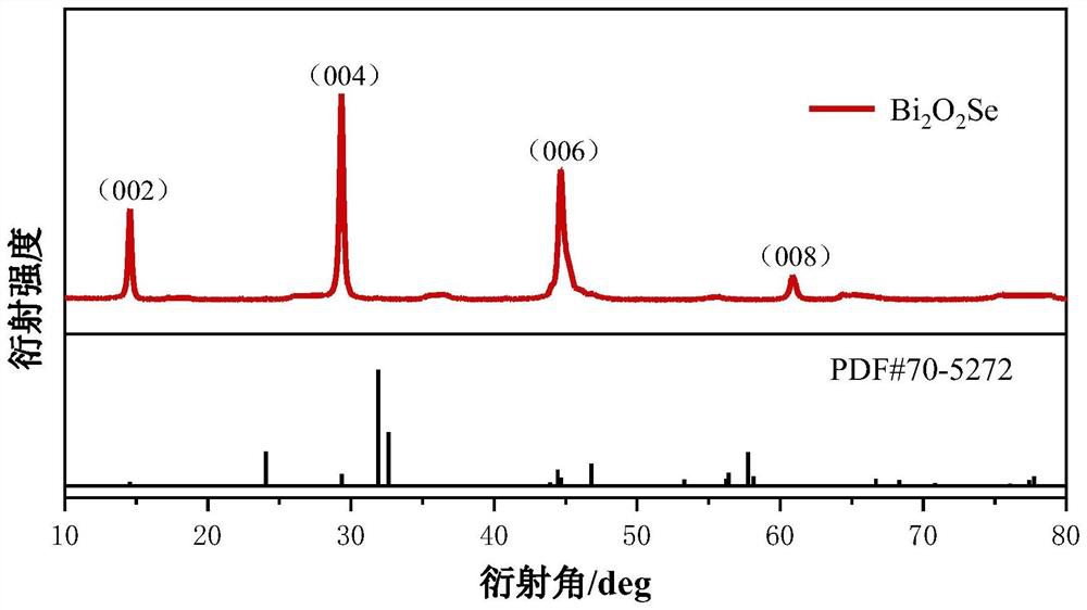
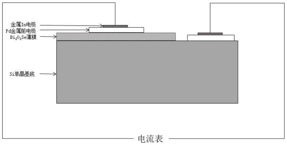
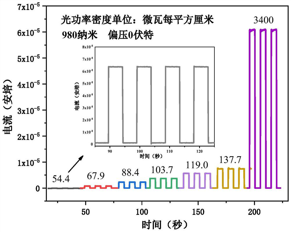

Image

  • Self-driven photoelectric detector based on Bi2O2Se thin film/Si heterojunction and preparation method thereof
  • Self-driven photoelectric detector based on Bi2O2Se thin film/Si heterojunction and preparation method thereof
  • Self-driven photoelectric detector based on Bi2O2Se thin film/Si heterojunction and preparation method thereof

Examples


Embodiment Construction

[0028] The invention utilizes spin coating, air annealing, chemical vapor deposition, wet transfer and other methods to prepare Bi on a Si semiconductor substrate 2 O 2 Se thin film layer, metal Pd front electrode is deposited by DC magnetron sputtering technology, metal In electrode is pressed and metal wire is connected to form a device. When exposed to light, due to the photoelectric effect and the presence of a built-in electric field, the device can exhibit significant response performance to light at an applied voltage of 0 volts.

[0029] The present invention will be described in detail below with reference to the embodiments and the accompanying drawings.

[0030] The present invention is a Bi-based 2 O 2 Self-driven photodetectors of Se thin films / Si heterojunctions including Bi 2 O 2 Se thin film layer and Si semiconductor substrate, Si substrate as Bi 2 O 2 The carrier for the Se film layer, Bi 2 O 2 The Se thin film layer is disposed on the surface of the...


PUM

PropertyMeasurementUnit
thicknessaaaaaaaaaa
thicknessaaaaaaaaaa
diameteraaaaaaaaaa

Abstract

The invention belongs to the technical field of optical detection, and particularly relates to a self-driven photoelectric detector which sequentially comprises a metal In point electrode, a metal Pd front electrode, a bismuth oxyselenide film layer and a silicon single crystal substrate from top to bottom. The bismuth oxyselenide thin film layer is prepared through a spin-coating method, air annealing treatment, chemical vapor deposition, wet transfer and the like. Test results show that the photoresponse performance of the bismuth oxyselenide-based device is greatly improved by constructing the heterojunction, and the device shows good self-driven photodetection performance.

Description

technical field [0001] The invention belongs to the technical field of light detection, and in particular relates to a self-driven photodetector and a preparation method thereof. Background technique [0002] In recent years, the booming optoelectronics industry has changed the world and entered every aspect of life. As one of the important optoelectronic devices, photodetectors have the ability to accurately convert optical signals into electrical signals, and are widely used in many fields including image sensing, defense communications, machine vision, environmental monitoring, biomedical equipment, and day and night surveillance. Applications. Layered Bismuth Selenide (Bi 2 O 2 Se) has excellent stability, tunable energy band structure, and high carrier mobility [Nature Nanotechnology, 2017, 12, 530], and is regarded as a competitor for the new generation of electronic devices. Hydrothermal synthesis is a simple and efficient method for large-scale preparation of 2D ...

Claims


Application Information

Patent Timeline
Patent Type & Authority Applications(China)
IPC IPC(8): H01L31/18C23C14/18C23C14/35C23C16/01C23C16/30C23C28/00H01L31/0392H01L31/109
CPCH01L31/109H01L31/18H01L31/0392C23C14/35C23C14/185C23C16/305C23C16/01C23C28/322C23C28/34Y02P70/50
Inventor 凌翠翠薛鑫傅嘉文冯冰心曹敏张拓姬洪光王敬尧
Owner CHINA UNIV OF PETROLEUM (EAST CHINA)
Learn More