Band-gap reference circuit and chip
A reference circuit and core circuit technology, applied in the direction of adjusting electrical variables, instruments, control/regulation systems, etc., to achieve the effect of simplifying design requirements, high reliability, and reducing reliability design requirements
- Summary
- Abstract
- Description
- Claims
- Application Information
AI Technical Summary
Problems solved by technology
Method used
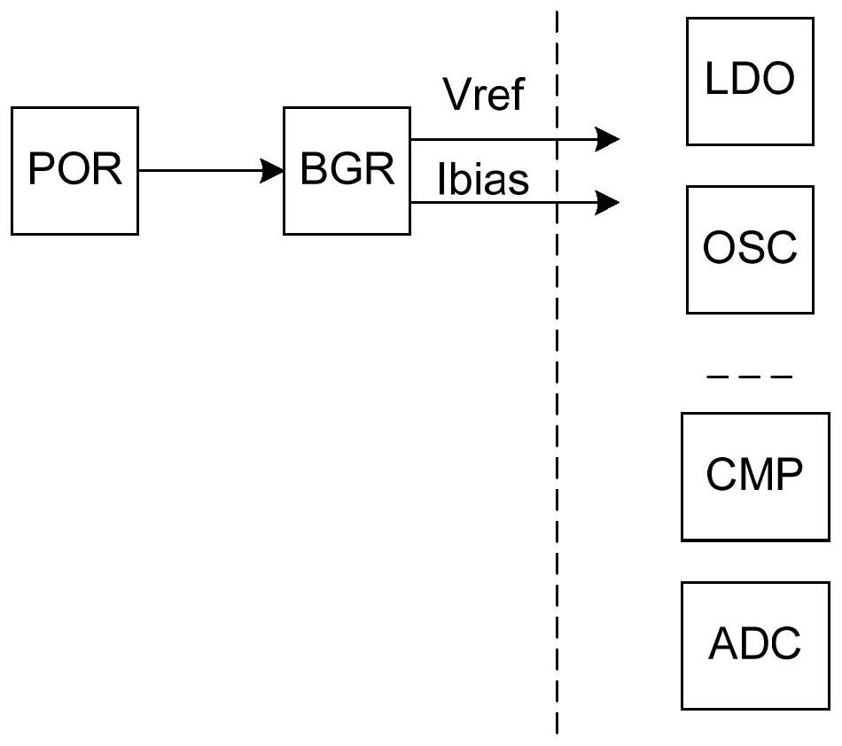
Image

Examples
Embodiment Construction
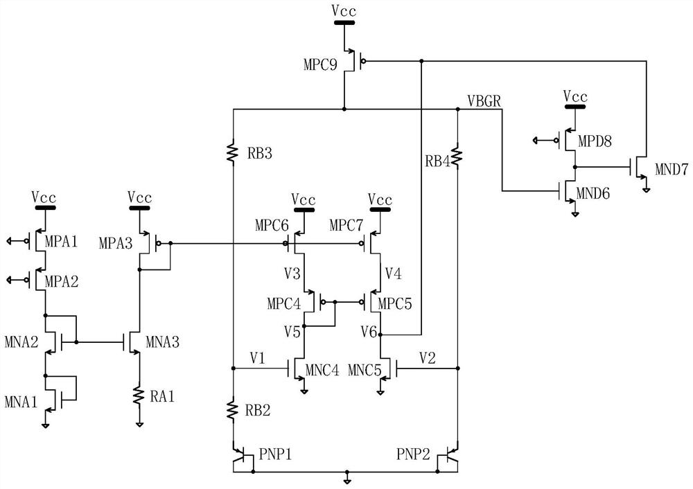
[0024] The operational amplifier bias circuit of the present invention adopts an NMOS tube as the operational amplifier input tube, and realizes a bandgap reference circuit with low operating voltage requirements, lower noise and high reliability by means of current biasing.
[0025] Bandgap reference circuit embodiment:
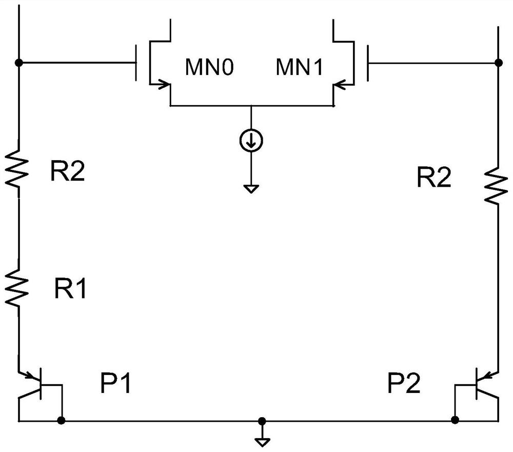
[0026]The bandgap reference circuit includes a bias current generating circuit, a bandgap core circuit, an operational amplifier bias circuit, and a start-up circuit. The operational amplifier bias circuit includes a feedback tube, an upper bias current source, a current mirror load, and an operational amplifier NMOS input tube; the bias current generation circuit is connected to the upper bias current source, the upper bias current source is connected to the current mirror load, and the current The mirror load is connected to the NMOS input tube of the operational amplifier, the NMOS input tube of the operational amplifier is connected to the bandgap core c...
PUM
 Abstract
Description
Claims
Application Information
 - Generate Ideas
- Intellectual Property
- Life Sciences
- Materials
- Tech Scout
- Unparalleled Data Quality
- Higher Quality Content
- 60% Fewer Hallucinations
Browse by: Latest US Patents, China's latest patents, Technical Efficacy Thesaurus, Application Domain, Technology Topic, Popular Technical Reports.
© 2025 PatSnap. All rights reserved.Legal|Privacy policy|Modern Slavery Act Transparency Statement|Sitemap|About US| Contact US: help@patsnap.com