Flexible ferroelectric film containing defect dipole and manufacturing method
A defect dipole, ferroelectric thin film technology, applied in thermoelectric devices, circuits, thermoelectric devices with thermal changes in dielectric constant, etc., can solve the problem of ferroelectric materials losing giant electric card effect, etc., and achieve a wide range of application prospects and markets. Effects of changing values of development space, surface flatness, high polarization
- Summary
- Abstract
- Description
- Claims
- Application Information
AI Technical Summary
Problems solved by technology
Method used
Image
Examples
Embodiment 1
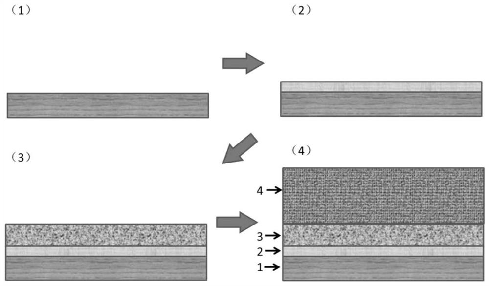
[0044]This embodiment discloses a flexible ferroelectric film containing defective dipoles, such as the attached figure 1 As shown, it includes: a mica substrate 1 , and a buffer layer 2 , a bottom electrode layer 3 and a ferroelectric functional layer 4 sequentially grown on the mica substrate 1 .
[0045] In order to further optimize the above technical solution, the material of the buffer layer 2 is CoFe 2 O 4 thin film with a thickness of 8 nm.
[0046] In order to further optimize the above technical solution, the material of the bottom electrode layer 3 is SrRuO 3 thin film with a thickness of 25 nm.
[0047] In order to further optimize the above technical solution, the material of the ferroelectric functional layer 4 is Pb (Zr 0.2 Ti 0.8 )O 3 thin film with a thickness of 240 nm.
Embodiment 2
[0049] On the basis of Embodiment 1, this embodiment discloses a method for manufacturing a flexible ferroelectric film containing defective dipoles, which specifically includes:
[0050] 1) A buffer layer is grown on a mica substrate by a pulsed laser deposition process;
[0051] Wherein, the smooth and flat mica substrate is selected; and the material of the buffer layer is CoFe 2 O 4 film;
[0052] 2) growing a bottom electrode layer on the buffer layer by a pulsed laser deposition process;
[0053] Among them, the material of the bottom electrode layer is SrRuO 3 film;
[0054] 3) growing a ferroelectric functional layer on the bottom electrode layer by a pulsed laser deposition process;
[0055] The material of the ferroelectric functional layer 4 is Pb (Zr 0.2 Ti 0.8 )O 3 film.
[0056] In order to further optimize the above-mentioned technical scheme, the laser in the pulsed laser deposition process used in the step 1) growing the buffer layer on the mica subst...
Embodiment 3
[0060] like figure 1 As shown, this embodiment discloses a flexible ferroelectric film containing defective dipoles, and the flexible ferroelectric thin film containing defective dipoles includes from bottom to top:
[0061] mica substrate 1; buffer layer 2 grown on mica substrate 1; bottom electrode layer 3 grown on buffer layer 2; ferroelectric functional layer 4 grown on bottom electrode layer 3.
[0062] In order to further optimize the above technical solution, the material of the buffer layer 2 is CoFe 2 O 4 thin film with a thickness of 12 nm.
[0063] In order to further optimize the above technical solution, the material of the bottom electrode layer 3 is SrRuO 3 thin film with a thickness of 35 nm.
[0064] In order to further optimize the above technical solution, the material of the ferroelectric functional layer 4 is Pb (Zr 0.2 Ti 0.8 )O 3 thin film with a thickness of 280 nm.
PUM
| Property | Measurement | Unit |
|---|---|---|
| Thickness | aaaaa | aaaaa |
| Thickness | aaaaa | aaaaa |
| Thickness | aaaaa | aaaaa |
Abstract
Description
Claims
Application Information
 - R&D
- Intellectual Property
- Life Sciences
- Materials
- Tech Scout
- Unparalleled Data Quality
- Higher Quality Content
- 60% Fewer Hallucinations
Browse by: Latest US Patents, China's latest patents, Technical Efficacy Thesaurus, Application Domain, Technology Topic, Popular Technical Reports.
© 2025 PatSnap. All rights reserved.Legal|Privacy policy|Modern Slavery Act Transparency Statement|Sitemap|About US| Contact US: help@patsnap.com


