
Circuit board with stepped blind holes

A ladder type, circuit board technology, applied in printed circuit, printed circuit manufacturing, printed circuit components, etc., can solve the problem that the working heat of the circuit board is easily piled up at the cross-linking place of the blind hole, the smooth surface of the circuit layer has insufficient impact resistance, Lack of circuit board substrate installation and adaptation capabilities to achieve the effect of improving assembly safety, improving relative physical strength, and ensuring installation and adaptation capabilities

Pending Publication Date: 2022-05-27
黄石永兴隆电子有限公司
View PDF0 Cites 0 Cited by
  • Summary
  • Abstract
  • Description
  • Claims
  • Application Information

AI Technical Summary

Problems solved by technology

[0004] The purpose of the present invention is: in order to solve the problem that some circuit holes and blind holes are mostly simple hole pile structures, the impact resistance of the smooth surface of the circuit layer is insufficient after electroplating, and its surface is easily broken due to external impact, which affects the conductive circuit, and then causes The connection accuracy between the inner and outer circuits, and the lack of installation and adaptation capabilities for the circuit board substrate, the overall working heat of the circuit board is easy to pile up at the cross-linking place of the blind hole, which affects the working accuracy of the final product, and a proposed Circuit boards with stepped blind vias

Method used


Image

  • Circuit board with stepped blind holes
  • Circuit board with stepped blind holes
  • Circuit board with stepped blind holes

Examples


Embodiment 1

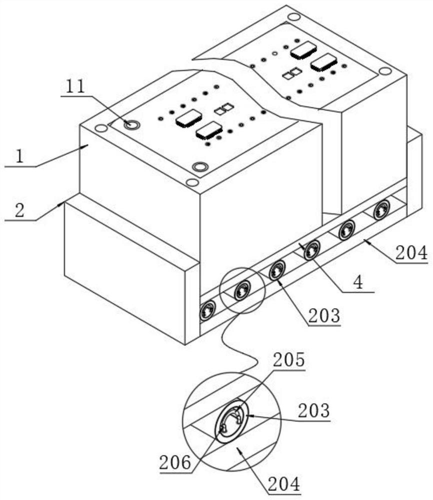
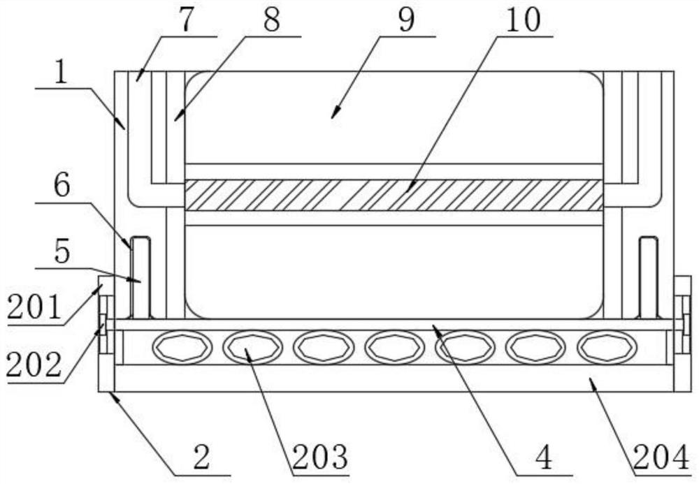
[0046] see Figure 1-7 As shown, the present invention provides a technical solution: a circuit board with stepped blind holes, comprising a circuit board main body 9 and an movably connected fixing frame 1 , the top of the circuit board main body 9 is provided with a number of stepped blind holes by laser. The blind hole mechanism 3, and the inner cavity of the stepped blind hole mechanism 3 is provided with a drainage channel 302, and the inner cavity of the stepped blind hole mechanism 3 is provided with a tapered groove 305, and the tapered groove 305 is coated with modified paint, The top of the circuit board main body 9 is embedded with a plurality of assembly sets 11 , the blind hole mechanism 3 includes a blind hole seat 301 , the blind hole seat 301 is cast on the top of the circuit board main body 9 , and the inner cavity of the blind hole seat 301 is punched and opened. There are three stepped holes 304, and the blind hole seat 301 has a tapered groove 305, and the ...

Embodiment 2

[0049] like Figure 5 As shown, the difference from Embodiment 1 is that the blind hole mechanism 3 includes a blind hole seat 301, and the inner cavity of the blind hole seat 301 is sequentially sleeved with three hole cavity sleeves 306 from top to bottom, and the blind hole seat Both sides of the top of 301 are provided with drainage channels 302, and the drainage channels 302 communicate with the corresponding position hole sleeve 306 through the branch hole 303, and the built-in diameter of the hole sleeve 306 decreases sequentially from top to bottom, and the hole sleeve 306 The inner cavity is coated with modified paint.

[0050] The specific embodiment is as follows: this embodiment mainly realizes the pre-assembly of the blind hole seat 301 through three mutually nested cavity sleeves 306, thereby effectively improving the assembly accuracy of the cavity sleeve 306 and realizing the size of the cavity sleeve 306. It can be prepared to meet the production and assembly...

Embodiment 3

[0052] like Figure 1-3 As shown in FIG. 6, a circuit board containing stepped blind holes includes a circuit board body 9 and a movably connected fixing frame 1. A number of stepped blind hole mechanisms 3 are opened on the top of the top of the circuit board body 9 by laser, and The inner cavity of the stepped blind hole mechanism 3 is provided with a drainage channel 302, and the inner cavity of the stepped blind hole mechanism 3 is provided with a tapered groove 305, and the tapered groove 305 is coated with modified paint, and the circuit board main body 9 A number of assembling sets 11 are embedded on the top, and an assembling mechanism 2 is slidably connected to the bottom of the fixing frame 1. The assembling mechanism 2 includes a sliding seat 201, one side of the sliding seat 201 is in contact with one side of the fixing frame 1, and the A sliding slot is provided on one side of the sliding seat 201, and a sliding block 202 is slidably connected in the sliding slot,...


PUM


Abstract

The invention discloses a circuit board with stepped blind holes, and belongs to the technical field of circuit boards, the circuit board comprises a circuit board main body and a movably connected fixing frame, the top of the circuit board main body is provided with a plurality of stepped blind holes through laser, the inner cavity of each stepped blind hole is provided with a drainage hole channel, and the inner cavity of each stepped blind hole is provided with a conical groove. In the invention, the stepped energy absorption arrangement of the electroplated layer is realized through the plurality of stepped hole cavities in the blind hole seat, the heat dissipation of the electroplating liquid and the blind hole can be realized through the branch holes and the liquid discharge hole channels, and the seepage of the percolate to the outside of the substrate is avoided through the stepped hole cavities; the relative physical strength of the blind hole seat is improved through permeation of percolate, the communication precision between an inner layer circuit and an outer layer circuit is improved, the bonding sealing performance of the circuit board bodies on the two sides is achieved through the bonding colloid, precise glue injection is achieved through the glue injection holes in the two sides, the installation adaptation capacity of the circuit board substrate is guaranteed, and the adaptation capacity to external impact is guaranteed.

Description

technical field [0001] The invention belongs to the technical field of circuit boards, and in particular relates to a circuit board containing stepped blind holes. Background technique [0002] The circuit board is the basic component of the integrated circuit through the miniaturization of the circuit. The circuit board realizes the full utilization of the circuit through the layout of the cushion layer. In order to connect the multi-layer circuit, it is generally necessary to use the electroplating process to connect the inner and outer layers of the conductive plating layer. deal with. [0003] Blind via is to connect the outermost circuit in the printed circuit board and the adjacent inner layer with plated holes. Since the opposite side cannot be seen, it is called blind via. The existing blind vias are mostly blind vias. The simple hole pile structure has insufficient impact resistance on the smooth surface of the circuit layer after electroplating, and its surface is...

Claims


Application Information

Patent Timeline
Patent Type & Authority Applications(China)
IPC IPC(8): H05K1/02H05K1/11H05K1/14H05K3/00H05K3/18
CPCH05K1/0271H05K1/021H05K1/115H05K1/14H05K3/0044H05K3/188Y02E60/10
Inventor 张顺义
Owner 黄石永兴隆电子有限公司
Learn More