Silicon carbide mosfet with integrated gated diode for high surge current capability

A gate-controlled diode and surge current technology, which is applied in the direction of high-efficiency power electronic conversion, circuits, electrical components, etc., can solve the problems of reducing the reliability of the gate oxide layer of gate-controlled diodes, so as to improve long-term reliability and reduce cell Effect of increased size and reduced switching loss

Active Publication Date: 2022-07-15
NOVUS SEMICON CO LTD
View PDF12 Cites 0 Cited by
  • Summary
  • Abstract
  • Description
  • Claims
  • Application Information

AI Technical Summary

Problems solved by technology

However, as the withstand voltage of silicon carbide power devices becomes higher and higher, the drift region becomes thicker and thicker, which makes more and more minority carriers recombine in the drift region to form a recombination current during the bipolar conduction process of the PIN. The current will all be borne by the channel of the gate-controlled diode, which will greatly reduce the reliability of the gate oxide layer of the gate-controlled diode

Method used


Image

  • Silicon carbide mosfet with integrated gated diode for high surge current capability
  • Silicon carbide mosfet with integrated gated diode for high surge current capability
  • Silicon carbide mosfet with integrated gated diode for high surge current capability

Examples


Embodiment Construction

[0031] The principles and features of the present invention will be described below with reference to the accompanying drawings. The examples are only used to explain the present invention, but not to limit the scope of the present invention.

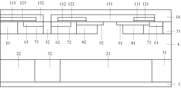
[0032] The cellular structure of the present invention is as figure 1 shown in figure 1 Each part includes backside metal 1, first N-type silicon carbide substrate 21, second N-type silicon carbide substrate 22, first P-type backside implant 31, second P-type backside implant 32, N-type silicon carbide epitaxy 4 , the first P-type source implant 51, the second P-type source implant 52, the first N-type source implant 61, the second N-type source implant 62, the third N-type source implant 63, the first P-type Well region 71, second P-type well region 72, third P-type well region 73, first P-type buried layer 81, second P-type buried layer 82, first N-type conduction layer 91, second N-type conduction layer Flow layer 92, N-type JFET i...


PUM


Abstract

The invention relates to a silicon carbide MOSFET with high anti-surge current capability and integrated gate-controlled diode, which belongs to the technical field of power semiconductor devices. As the withstand voltage of silicon carbide power devices becomes higher and higher, the drift region becomes thicker and thicker, which makes more and more minority carriers recombine in the drift region during the bipolar conduction process of the PIN to form a recombination current. It will all be borne by the channel of the gated diode, which will greatly reduce the reliability of the gate oxide layer of the gated diode. In order to alleviate this problem, a parallel PNP BJT is integrated for the gated diode, and the reverse-biased PN junction is used to reduce the effective base region thickness and reduce the recombination of minority carriers in the base region, that is, reduce the generation of recombination current and alleviate the wave The current density of the channel region in the surge state improves the overall surge current resistance capability of the device.

Description

technical field [0001] The invention belongs to the technical field of power semiconductor devices, in particular to a silicon carbide MOSFET with integrated gate-controlled diode with high anti-surge current capability. Background technique [0002] The wide-bandgap semiconductor material SiC is an ideal material for the preparation of high-voltage power electronic devices. Compared with Si material, SiC material has a high breakdown electric field strength (4×10 6 V / cm), high carrier saturation drift velocity (2×10 7 cm / s), high thermal conductivity, good thermal stability, etc., so it is especially suitable for high-power, high-voltage, high-temperature and radiation-resistant electronic devices. [0003] SiC VDMOS is a commonly used device in SiC power devices. Compared with bipolar devices, since SiCVDMOS has no charge storage effect, it has better frequency characteristics and lower switching losses. At the same time, the wide band gap of SiC material enables the ope...

Claims


Application Information

Patent Timeline
Patent Type & Authority Patents(China)
IPC IPC(8): H01L29/78H01L29/739H01L29/06H01L29/16
CPCH01L29/7803H01L29/7391H01L29/0684H01L29/1608Y02B70/10
Inventor 顾航高巍戴茂州
Owner NOVUS SEMICON CO LTD
Why Eureka
Try Eureka