


Quick Research
Generate reliable direction feasibility study reports for your R&D in just a few steps.

Technical Q&A
Discover and master advanced knowledge NOW. Basics, ideas, possibilities, all at once.

Find Solutions
As an expert in R&D theories, this can generate solutions to your technical problems instantly.

Evaluate Feasibility
Analyze your overall solution with one click, know your potential R&D risks in advance.

Monitor Landscape
Get weekly tech updates, stay abreast of the latest tech innovations and key insights.
Memory verification unit, method and chip
A memory and sub-unit technology, applied in the computer field, can solve problems such as complex design and limited memory architecture, and achieve the effects of simple implementation, low implementation cost, and high data security level
- Summary
- Abstract
- Description
- Claims
- Application Information
AI Technical Summary
Problems solved by technology
Method used
Image

Examples
Embodiment 1
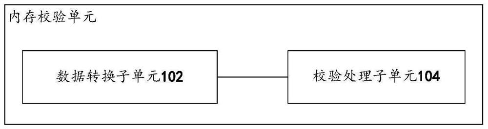
[0023] Based on the bus system, a memory check unit in the embodiment of the present application is as follows: Figure 2A As shown, it includes: a data conversion subunit 102 and a check processing subunit 104 .
[0024] in:
[0025] The data conversion subunit 102 is configured to receive the first transmission data transmitted from the bus to the memory controller, and convert the first transmission data into parity bit width data, wherein the bit width of the parity bit width data is the bus bit width half of .
[0026] The check processing sub-unit 104 is used for inserting check data with the same number of bits as the number of bytes in each check bit width data in every other byte to form a second check data with the same number of bits as the bus bit width. transfer data; send second transfer data to the memory controller.
[0027] In this embodiment, the bus may be a high-bandwidth bus, such as AHB or ASB or AXI in an AMBA bus. Therefore, the memory verification ...
Embodiment 2
[0041] refer to image 3 , showing a flow chart of steps of a memory verification method according to Embodiment 2 of the present application.
[0042] The memory verification method of this embodiment can be implemented by the aforementioned memory verification unit, and the memory verification method of this embodiment includes the following steps:
[0043] Step S202: Receive the first transmission data transmitted to the memory controller from the bus, and convert the first transmission data into parity bit width data.
[0044] The solution of this embodiment can be applied to the system-on-chip of the AMBA bus protocol, especially the high-bandwidth bus, including but not limited to the AXI bus.
[0045] After the memory check unit receives the first transmission data transmitted from the bus, it can convert it into check bit width data, wherein the bit width of the check bit width data is half of the bus bit width. Optionally, the first transmission data may be converte...
Embodiment 3
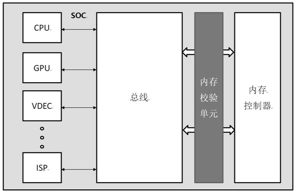
[0064] refer to Figure 4 , showing a schematic structural diagram of a chip according to Embodiment 3 of the present application.
[0065] The chip in this embodiment at least includes: a processor, a bus, a memory, a memory controller, and the memory check unit described in the first embodiment; wherein: the memory controller is connected between the processor and the memory through a bus; The memory check unit is arranged at the interface of the memory controller.
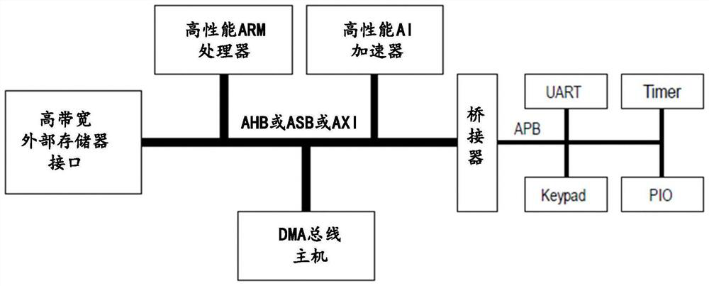
[0066] In a specific example, as Figure 4 shown, the chip is based on the AMAB bus structure, which in addition to including figure 1 In addition to the high-performance central bus, processor, on-chip memory interface (high-bandwidth external memory interface, used to access on-chip memory), high-performance AI accelerator, DMA, bridge and APB shown in The described kernel check unit and kernel controller.
[0067] It can be seen from the figure that the kernel controller is connected between the on-chip m...
PUM
 Abstract
Description
Claims
Application Information
 - R&D Engineer
- R&D Manager
- IP Professional
- Industry Leading Data Capabilities
- Powerful AI technology
- Patent DNA Extraction
Browse by: Latest US Patents, China's latest patents, Technical Efficacy Thesaurus, Application Domain, Technology Topic, Popular Technical Reports.
© 2024 PatSnap. All rights reserved.Legal|Privacy policy|Modern Slavery Act Transparency Statement|Sitemap|About US| Contact US: help@patsnap.com