P-type PIN diode adopting InGaN and preparation method thereof
A PIN diode and diode technology, applied in the field of electronic devices, can solve the problems affecting the performance of GaNPIN diodes, difficult to achieve high-quality heavy doping, low effective doping concentration, etc., to improve device performance, reduce number, and high hole concentration. Effect
- Summary
- Abstract
- Description
- Claims
- Application Information
AI Technical Summary
Problems solved by technology
Method used
Image
Examples
Embodiment 1
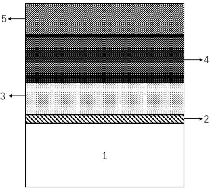
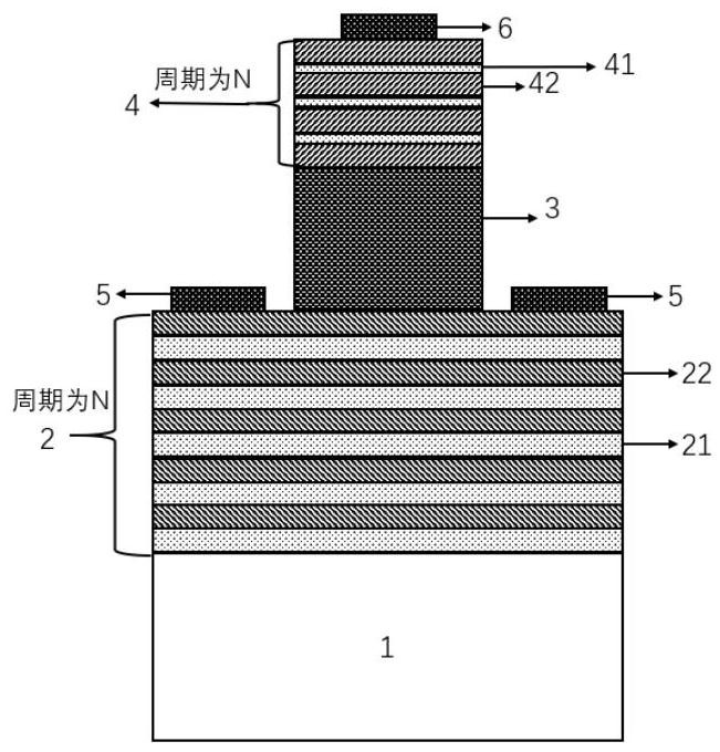
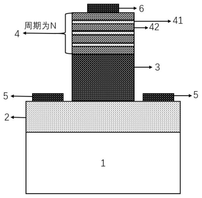
[0068] Embodiment 1, the N-type layer is prepared on a sapphire substrate as a GaN layer and Al with a thickness of 5nm 0.2 Ga 0.8 5 layers of N are alternately arranged periodically, and the interlayer doping is 1×10 16 cm -3 , the layer-to-layer interface doping concentration is 1×10 20 cm -3 ; The intrinsic layer is Al whose composition coefficient x varies from 0 to 0.4, and linearly decreases from the N-type layer to the P-type layer. x Ga 1-x N layer with a thickness of 10 nm and a doping concentration of 1 × 10 14 cm -3 ; P-type layers are GaN layers with a thickness of 1 nm and In layers with a thickness of 10 nm 0.2 Ga 0.8 N is arranged alternately in 5 cycles, and In 0.2 Ga 0.8 The N layer is doped to a hole concentration of 1×10 17 cm -3 PIN diode.
[0069] Step 1, epitaxial growth of N-type multi-channel, such as Figure 4 (a)-4(d).
[0070] 1.1) Using the MOCVD method, epitaxially grow a layer with a thickness of 5 nm and a doped Si concentration of...
Embodiment 2
[0086] Example 2, the N-type layers are prepared on the Si substrate as a GaN layer with a thickness of 30 nm and an Al 0.3 Ga 0.7 The N layers are alternately arranged in 30 cycles, and the interlayer doping is 5×10 17 cm -3 , the layer-to-layer interface doping concentration is 1×10 20 cm -3 ; The intrinsic layer is Al whose composition coefficient x varies from 0 to 0.6, and linearly decreases from the N-type layer to the P-type layer. x Ga 1-x N layer with a thickness of 20 μm and a doping concentration of 5×10 15 cm -3 ; P-type layers are GaN layers with a thickness of 50 nm and In layers with a thickness of 500 nm 0.3 Ga 0.7 The N layers are alternately arranged in 4 cycles, and In 0.3 Ga 0.7 The N layer is doped to a hole concentration of 5×10 19 cm -3 PIN diode.
[0087] Step 1, epitaxial growth of N-type multi-channel, such as Figure 4 (a)-4(d).
[0088] 1a) Using the MOCVD method, a layer with a thickness of 20 nm and a doped Si concentration of 5 × 1...
Embodiment 3
[0104] Example 3, the preparation substrate is SiC, the N-type layer is a GaN layer with a thickness of 60 nm and an Al with a thickness of 40 nm 0.4 Ga 0.6 The N layers are arranged alternately in cycles, the number of cycles is 50, and the interlayer doping is 5×10 18 cm -3 , the layer-to-layer interface doping concentration is 1×10 20 cm -3 , the intrinsic layer is Al with a thickness of 100 μm and the composition coefficient x varies from 0 to 0.8, and linearly decreases from the N-type layer to the P-type layer. x Ga 1-x N layer with a doping concentration of 1×10 17 cm -3 , the P-type layer is a GaN layer with a thickness of 200 nm and an In layer with a thickness of 1 μm 0.4 Ga 0.6 The N layers are arranged alternately with a period of 5, and In 0.4 Ga 0.6 The N layer is doped to a hole concentration of 1×10 21 cm -3 PIN diode.
[0105] Step A, epitaxial growth of N-type multi-channel, such as Figure 4 (a)-4(d).
[0106] A1) Using the MOCVD method, a lay...
PUM
| Property | Measurement | Unit |
|---|---|---|
| thickness | aaaaa | aaaaa |
| thickness | aaaaa | aaaaa |
| thickness | aaaaa | aaaaa |
Abstract
Description
Claims
Application Information
 - R&D Engineer
- R&D Manager
- IP Professional
- Industry Leading Data Capabilities
- Powerful AI technology
- Patent DNA Extraction
Browse by: Latest US Patents, China's latest patents, Technical Efficacy Thesaurus, Application Domain, Technology Topic, Popular Technical Reports.
© 2024 PatSnap. All rights reserved.Legal|Privacy policy|Modern Slavery Act Transparency Statement|Sitemap|About US| Contact US: help@patsnap.com


