


Quick Research
Generate reliable direction feasibility study reports for your R&D in just a few steps.

Technical Q&A
Discover and master advanced knowledge NOW. Basics, ideas, possibilities, all at once.

Find Solutions
As an expert in R&D theories, this can generate solutions to your technical problems instantly.

Evaluate Feasibility
Analyze your overall solution with one click, know your potential R&D risks in advance.

Monitor Landscape
Get weekly tech updates, stay abreast of the latest tech innovations and key insights.
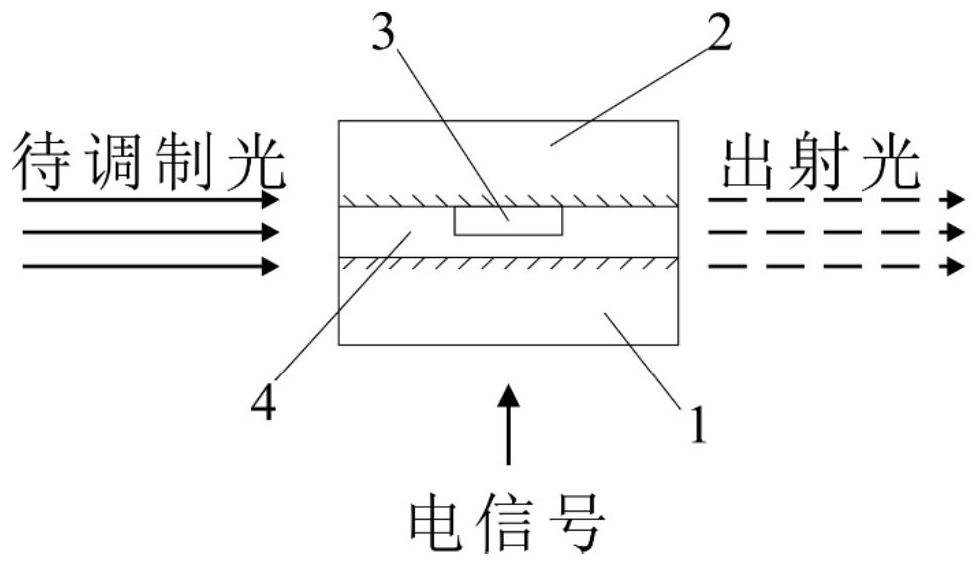
Ultrafast electro-optical modulation device and method
An electro-optical modulation and ultra-fast technology, applied in the field of communication, can solve the problems of only barely reaching terahertz, limiting the response speed of the modulator, high power consumption, etc., achieving the effect of easy secondary design, good modulation effect, and simple composition.
- Summary
- Abstract
- Description
- Claims
- Application Information
AI Technical Summary
Problems solved by technology
Method used
Image

Examples
example 1
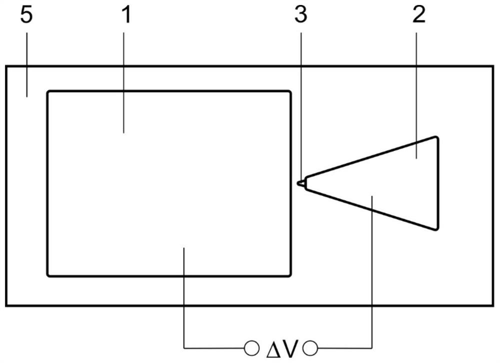
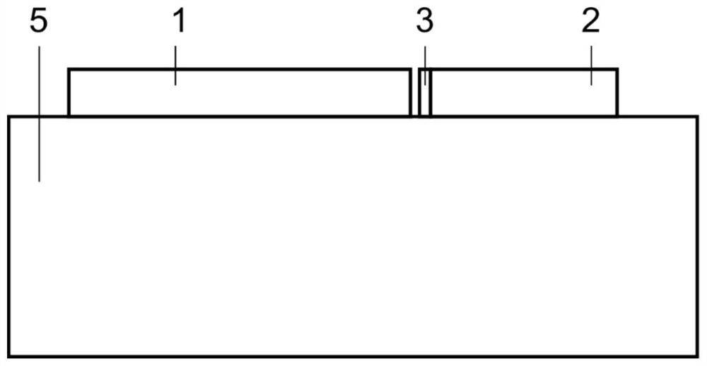
[0043] Example 1: An electro-optic modulator with ultra-fast modulation speed, one of the structures is a flat two-dimensional structure, and its composition is as follows figure 2 and image 3 As shown, it includes a conductor 1 , another conductor 2 , and a nanoscale conductor 3 seamlessly electrically connected to 2 , and conductors 1 , 2 , and 3 are all located on a dielectric substrate 5 . Use external instruments to apply modulation signals, such as external electrodes, so that there is a potential difference of ΔV between conductors 1 and 2. By controlling the level of the potential difference ΔV, the carrier density distribution of the nanometer-sized conductive material structure 3 will be significantly changed, thereby causing the localized spatial light field distribution properties near the surface of the structure 3 to change accordingly. The localized near-field is still not directly perceivable by external detectors. Furthermore, the composition materials and...
example 2
[0044] Example 2: An electro-optic modulator with ultra-fast modulation speed, one of its structures only needs one piece of conductor, its front view and side view are as follows Figure 4 and Figure 5 As shown, conductors 1 and 3 are seamlessly electrically connected. Based on the same principle as in Example 1, a background electric field given by a modulation signal source in the area surrounded by the dotted line acts as a modulation signal to affect the carrier density distribution of the micro-nano conductive structure 3, thereby affecting the properties of the output light, and finally achieves the modulation. Effect.
example 3
[0045] Example 3: An electro-optic modulator with ultra-fast modulation speed, the other structure is a three-dimensional rotationally symmetrical three-dimensional structure, such as Figure 6 As shown, the cross-sectional view of the plane where the axis of symmetry is located is shown in Figure 7 , including a conductor 1, another conductor 2, a nanoscale conductive material structure 3 seamlessly electrically connected to the 2, and an insulating medium 4 filled between the conductors. According to the same principle and operation steps as Example 1, this device structure can also realize electro-optic modulation.
[0046] In order to clearly demonstrate the modulation effect and response speed of the modulator device designed based on the modulation method in the present invention, we performed numerical simulation on Example 3, and estimated its modulation contrast and response time. The modulation contrast can be calculated according to the scattering cross section σ ...
PUM
| Property | Measurement | Unit |
|---|---|---|
| capacitance | aaaaa | aaaaa |
Abstract
Description
Claims
Application Information
 - R&D Engineer
- R&D Manager
- IP Professional
- Industry Leading Data Capabilities
- Powerful AI technology
- Patent DNA Extraction
Browse by: Latest US Patents, China's latest patents, Technical Efficacy Thesaurus, Application Domain, Technology Topic, Popular Technical Reports.
© 2024 PatSnap. All rights reserved.Legal|Privacy policy|Modern Slavery Act Transparency Statement|Sitemap|About US| Contact US: help@patsnap.com