Contact electrode preparation method, Mico-LED array device and preparation method thereof
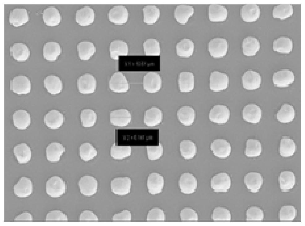
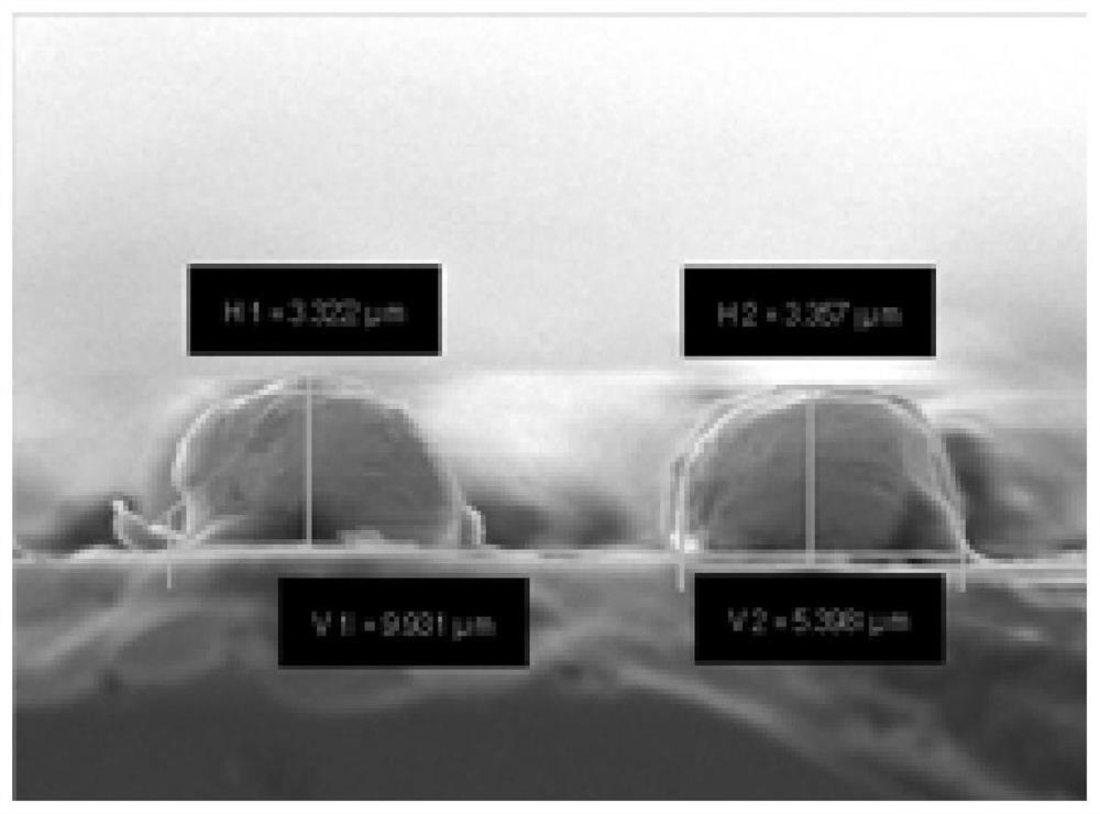
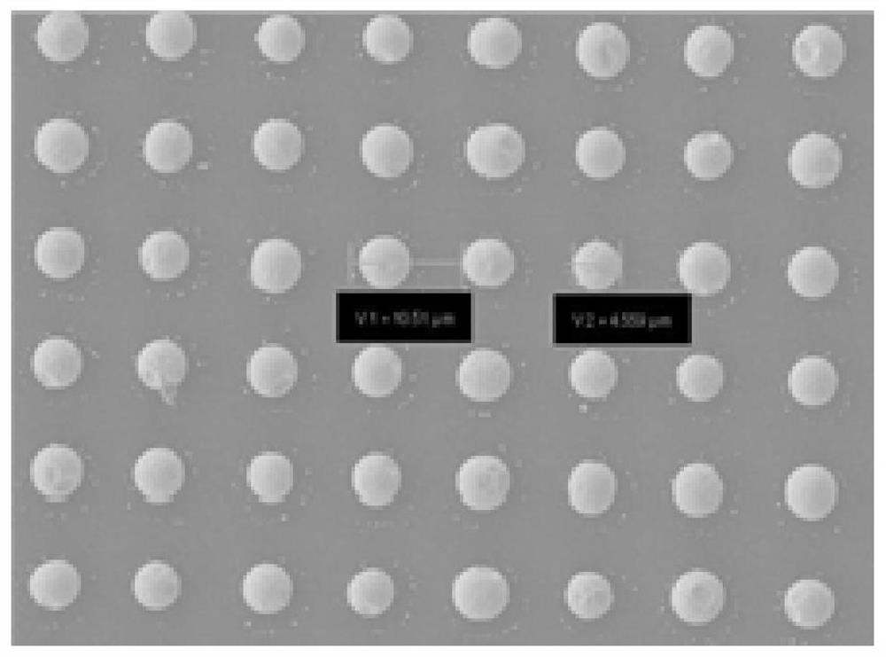
A technology of contact electrodes and arrays, which is applied in the field of Micro-LEDs, can solve the problems of inhomogeneous polycondensation of indium contact electrodes, large deviation, height of indium ball bumps, and uneven shape and size, and achieve uniform shape, reduced short circuit, and uniform size Effect
- Summary
- Abstract
- Description
- Claims
- Application Information
AI Technical Summary
Problems solved by technology
Method used
Image
Examples
preparation example Construction
[0033] reference Figures 11 to 14 , the present invention discloses a method of preparing an electrode, comprising the following steps:
[0034] Step 1: The Micro-LED array substrate 100 is provided, the contact electrode 200 position of the Micro-LED array substrate 100 is formed at the indium body layer 210.
[0035] Step 2: A metal protective layer 220 is formed on the indium body layer 210.
[0036] Step 3: The indium body layer 210 and the metal protective layer 220 are refluxed to obtain a contact electrode 200.
[0037] The present invention by providing a metal protective layer 220, a metal protective layer 220 for indium main layer 210 is isolated from air before reflux, protecting the indium main layer 210 from oxidation, avoiding the formation of an oxide layer affecting the effect of reflux into a ball, and protecting the indium main layer 210 during the reflux process does not occur climbing and forming whiskers, and to avoid evaporation and volatilization of the indi...
Embodiment 1
[0056]Micro-LED array substrate 100 may be prepared using any available method, reference Figures 9 to 16 In the present embodiment, the micro-LED array substrate 100 preparation method comprises the following steps:
[0057] Step S11: Refer to Figure 9 , in turn growing epitaxial flakes on the substrate 110, the epitaxial flakes comprise an N-type layer 1211, an active layer 1212 and a P-type layer grown sequentially on the substrate 110, in this particular embodiment, in order to improve the growth quality of the epitaxial flakes, before forming an epitaxial flake, further comprising the process of growing a buffer layer 150 on the substrate 110. In the present embodiment, in order to improve the growth quality of the epitaxial flakes, there is also a layer of u-GaN layer 160 growing above the buffer layer 150.
[0058] The material of the substrate 110 may be sapphire or silicon carbide, etc., in the present embodiment, the material of the substrate 110 is a sapphire transpare...
PUM
| Property | Measurement | Unit |
|---|---|---|
| thickness | aaaaa | aaaaa |
| electrical resistivity | aaaaa | aaaaa |
| electrical resistivity | aaaaa | aaaaa |
Abstract
Description
Claims
Application Information
 - R&D Engineer
- R&D Manager
- IP Professional
- Industry Leading Data Capabilities
- Powerful AI technology
- Patent DNA Extraction
Browse by: Latest US Patents, China's latest patents, Technical Efficacy Thesaurus, Application Domain, Technology Topic, Popular Technical Reports.
© 2024 PatSnap. All rights reserved.Legal|Privacy policy|Modern Slavery Act Transparency Statement|Sitemap|About US| Contact US: help@patsnap.com


