
Modeling method of field effect transistor

A field effect transistor and modeling method technology, applied in special data processing applications, instruments, design optimization/simulation, etc., can solve the problem of incomplete test data, no large-scale promotion, non-conservation of high-order current and charge sources, etc. problems, to save manpower and material resources, achieve coordinated development, and accelerate process optimization.

Pending Publication Date: 2022-04-22
KUNSHAN HUATAI ELECTRONICS TECH CO LTD
View PDF0 Cites 1 Cited by
  • Summary
  • Abstract
  • Description
  • Claims
  • Application Information

AI Technical Summary

Problems solved by technology

In some literatures, high-order current sources and charge sources are used to describe the NQS phenomenon, but some problems will be encountered in actual operation, such as the non-conservation of high-order current and charge sources, and incomplete test data. The environment has not been promoted on a large scale

Method used


Image

  • Modeling method of field effect transistor
  • Modeling method of field effect transistor
  • Modeling method of field effect transistor

Examples


Embodiment Construction

[0058] As mentioned earlier, some existing FET models, such as the Root Model and NeuroFET developed by Keysight, have covered the first-generation semiconductors to the third-generation semiconductors, such as MOSFET, LDMOS, GaAS pHEMT and GaN HEMT . These model architectures have nothing to do with the physics of the device. You only need to test standard S-parameters (scattering parameters), pulse or static I-V curves, and the models can be automatically generated without manual intervention. However, the biggest defect is that they do not model NQS well However, the model proposed by NXP and others uses high-order current sources and voltage sources, which can only simulate the NQS effect in a narrow band, and the charge conservation and simulation convergence of high-order sources will also be a major challenge.

[0059] In view of these deficiencies in the prior art, the inventors of the present application conducted an in-depth analysis of the NQS phenomenon of FETs, an...


PUM


Abstract

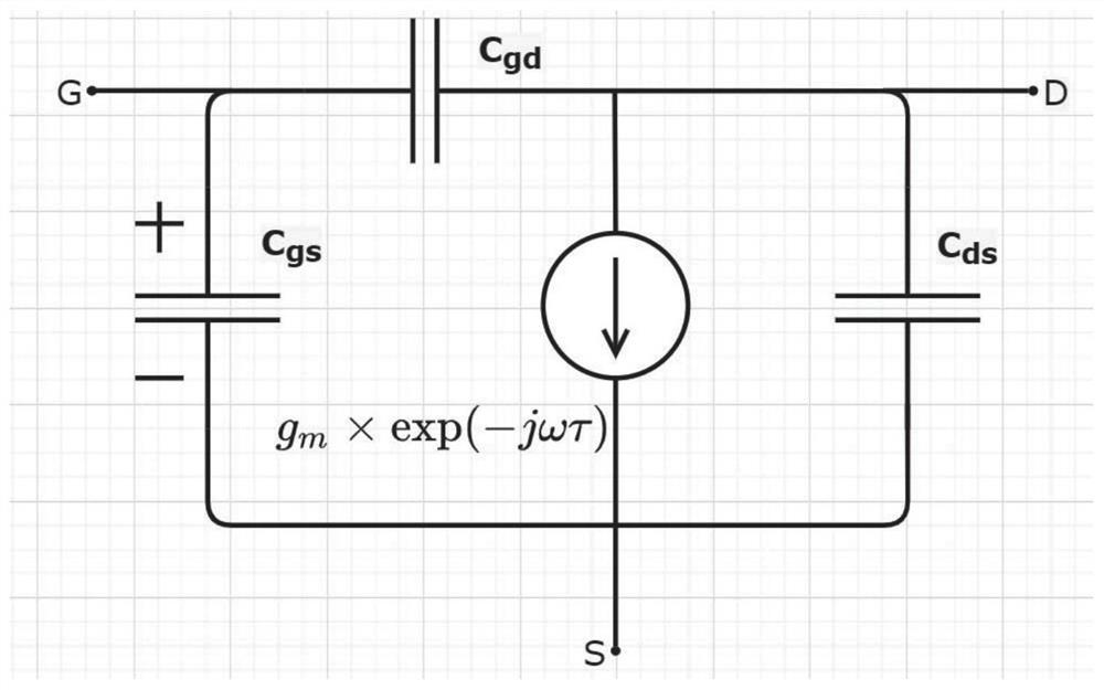
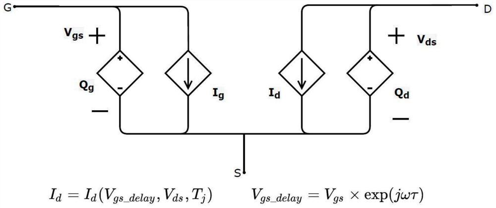
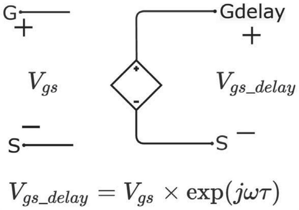
The invention discloses a modeling method of a field effect transistor, which comprises the following steps: establishing a small signal intrinsic part equivalent circuit of an FET (Field Effect Transistor), and obtaining a relationship between an internal intrinsic parameter and an external bias; constructing a large signal model of the FET, wherein the large signal model comprises a gate charge source, a drain charge source, a gate current source, a drain current source and an NQS sub-circuit; performing path integration on the port voltage to obtain a relation among the nonlinear current source, the charge source and the port voltage; and then a neural network analysis model can be obtained through storage in a lookup table mode or through neural network training. In the integration process of the current source and the charge source, the NQS effect is completely eliminated, the modeling mode is consistent with the physical mechanism of the NQS, unification of a small signal model and a large signal model is ensured, the precision of the model is not influenced by a frequency band, a high-order source does not need to be used, and in terms of robustness and precision of the model and the difficulty of model extraction, the modeling efficiency is greatly improved. And the model framework is obviously superior to the existing model framework.

Description

technical field [0001] The application relates to a field effect transistor (FET), in particular to a modeling method of the field effect transistor, which belongs to the field of integrated circuit design. Background technique [0002] In the 21st century, the information industry is developing rapidly. In just 20 years, the communication standard has spanned from 2G to 3G, 4G, and now to 5G. High capacity and low latency are the core of 5G communication, and high frequency and high power amplifier is one of the keys to achieve these two goals. As we all know, the distributed effects of high-frequency chips and the electromagnetic and thermal effects introduced by packaging make chip design and debugging extremely complicated. Therefore, the design process based on EDA (Electronic Design Automation) is extremely critical, and an accurate transistor RF nonlinear model is the key. The most complex and important part of a process. [0003] There are several types of RF trans...

Claims


Application Information

Patent Timeline
Patent Type & Authority Applications(China)
IPC IPC(8): G06F30/33G06F30/27
CPCG06F30/33G06F30/27G06F30/337
Inventor 黄安东
Owner KUNSHAN HUATAI ELECTRONICS TECH CO LTD
Learn More