Semiconductor device forming method and semiconductor device

A semiconductor and device technology, applied to the formation method of semiconductor devices and the field of semiconductor devices, can solve problems such as difficult control, increased electric field strength, and reduced yield

Active Publication Date: 2022-04-12
GUANGZHOU CANSEMI TECH INC
View PDF5 Cites 2 Cited by
  • Summary
  • Abstract
  • Description
  • Claims
  • Application Information

AI Technical Summary

Problems solved by technology

[0002] As the size of semiconductor devices (such as MOSFETs) continues to shrink, the channel length, polysilicon gate thickness, and junction depth of semiconductor devices are also reduced proportionally, but the power supply voltage is not reduced proportionally, which makes the electric field in the channel region The intensity increases significantly, and the hot carrier injection (Hot Carrier Injection, HCI) effect reduces the lifetime of semiconductor devices
[0003] In related technologies, HCI can be improved by adding lightly doped source and drain (Lightly Doped Drain, LDD) regions, but this method needs to add a new mask; or do not add a new mask but share the mask of other steps, And the LDD area is made by controlling the concentration, angle, and area of ​​the implanted area in the LDD area, but the control is difficult and the yield rate is reduced.
[0004] The increase of photomask or the decrease of yield rate will increase the production cost of semiconductor devices

Method used


Image

  • Semiconductor device forming method and semiconductor device
  • Semiconductor device forming method and semiconductor device
  • Semiconductor device forming method and semiconductor device

Examples


Embodiment 1

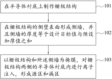
[0086] Including the following steps:

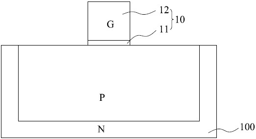
[0087] 201. Clean the semiconductor substrate, and fabricate a gate structure on the semiconductor substrate.

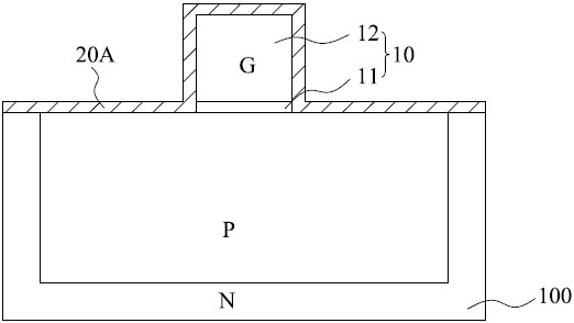
[0088] 202. Using the furnace tube atomic deposition process, grow the first silicon dioxide at 680°C, the first silicon dioxide covers the side and top surfaces of the gate structure and the top surface of the semiconductor substrate outside the gate structure, and the second The thickness of silicon dioxide is equal to the sum of the design target value of 150 Å and the preset thickening value of 150 Å, that is, 300 Å.

[0089] 203. A furnace tube atomic deposition process is used to grow silicon nitride on the surface of the first silicon dioxide at 650° C., with a growth thickness of 300 Å.

[0090] 204. A furnace tube atomic deposition process is used to grow second silicon dioxide on the surface of silicon nitride at 680° C., with a growth thickness of 1000 Å.

[0091] 205. Dry etching is used to etch the second silicon...

Embodiment 2

[0095] Including the following steps:

[0096] 301. Clean the semiconductor substrate, and fabricate a gate structure on the semiconductor substrate.

[0097] 302. Using a chemical vapor deposition process, grow first silicon dioxide, the first silicon dioxide covers the side and top surfaces of the gate structure and the top surface of the semiconductor substrate outside the gate structure, and the first silicon dioxide The thickness is equal to the sum of the design target value of 100 Å and the preset thickening value of 100 Å, that is, 200 Å.

[0098] 303. Using a low-pressure chemical vapor deposition process, silicon nitride is grown on the surface of the first silicon dioxide to a thickness of 500 Å.

[0099] 304 . Dry etching is used to etch the silicon nitride in the target etching area and the first silicon dioxide of 40 Å to form a second sub-sidewall, and the second sub-sidewall is silicon nitride. Wherein, the target etching area includes the top surface of the ...


PUM

PropertyMeasurementUnit
thicknessaaaaaaaaaa
thicknessaaaaaaaaaa

Abstract

The invention discloses a forming method of a semiconductor device and the semiconductor device. The forming method comprises the following steps: manufacturing a gate structure on a semiconductor substrate; forming a side wall on the surface of the side wall of the gate structure, wherein the thickness of the side wall is equal to the sum of a design target value and a preset thickening value; and performing ion implantation in the semiconductor substrate at two sides of the gate structure by taking the gate structure and the side walls as masks to form a source region and a drain region. By thickening the side wall of the gate structure, the distance between the source and the drain of the semiconductor device is increased, so that the electric field peak value in a channel can be reduced, the HCI effect is improved, the method is simple to operate, and the cost is basically not increased.

Description

technical field [0001] The present application relates to the technical field of semiconductor devices, in particular to a method for forming a semiconductor device and the semiconductor device. Background technique [0002] As the size of semiconductor devices (such as MOSFETs) continues to shrink, the channel length, polysilicon gate thickness, and junction depth of semiconductor devices are also reduced proportionally, but the power supply voltage is not reduced proportionally, which makes the electric field in the channel region The intensity increases obviously, and the hot carrier injection (Hot Carrier Injection, HCI) effect reduces the lifetime of semiconductor devices. [0003] In related technologies, HCI can be improved by adding lightly doped source and drain (Lightly Doped Drain, LDD) regions, but this method needs to add a new mask; or do not add a new mask but share the mask of other steps, The LDD region is manufactured by controlling the ion implantation co...

Claims


Application Information

Patent Timeline
Patent Type & Authority Applications(China)
IPC IPC(8): H01L21/336H01L29/423H01L29/78
Inventor 石卓李玉科
Owner GUANGZHOU CANSEMI TECH INC
Why Eureka
Try Eureka