Optical waveguide type light combiner and projection device using same

An optical waveguide and waveguide technology, applied in the field of optical projection display, can solve the problems of weak confinement, large optical path size, low refractive index, etc., and achieve the effect of strong confinement ability, small bending radius and simple structure

Pending Publication Date: 2022-04-05
苏州龙马璞芯芯片科技有限公司
View PDF0 Cites 2 Cited by
  • Summary
  • Abstract
  • Description
  • Claims
  • Application Information

AI Technical Summary

Problems solved by technology

[0006] (1) Dichroic mirrors combine light. This light combination method has high efficiency, but the assembly process is complicated and the size of the optical path is large, which is not conducive to mass production and miniaturization of the system
[0007] (2) Prism combined light, this light combined method has high efficiency, and the assembly process is complicated and relatively simplified, but the size of the optical path is large, which is not conducive to the miniaturization of the system
[0008] (3) PLC silica waveguide combined light, which can achieve high efficiency, but due to the weak limitation of the silica waveguide core layer on light (low relative refractive index, , n core is the core refractive index, n clad is the cladding refractive index), the bending radius needs to be very large, resulting in a larger size of the entire light-combining device, and the coupling design is more complicated, including three separate coupling regions, which further increases the device length, making the total length exceed 10 mm

Method used


Image

  • Optical waveguide type light combiner and projection device using same
  • Optical waveguide type light combiner and projection device using same
  • Optical waveguide type light combiner and projection device using same

Examples


Embodiment 1

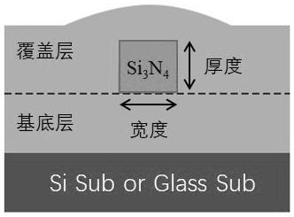
[0055] Schematic diagram of the optical waveguide section figure 1 As shown, there is a layer of SiO on a silicon wafer or glass substrate 2 The base layer has a thickness of 2 μm; the core layer of the optical waveguide is Si 3 N 4 , its thickness and width are both 0.16 μm; there is SiO on top 2 As a covering layer to ensure the reliability of the waveguide. The cladding layer (including the base layer and the cladding layer, which are made of the same material in this embodiment) and the refractive index of the core layer of the optical waveguide are shown in Table 1.

[0056] Table 1 Cladding and core refractive index of optical waveguide

[0057]

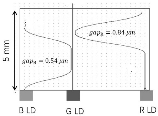
[0058] refer to figure 2 As shown, the red, green, and blue monochromatic laser beams respectively enter the three optical waveguides through the coupler, and the blue light wavelength is 450 nm, which is generated by a GaN-based semiconductor laser and enters the leftmost optical waveguide (this embodiment The middle...

Embodiment 2

[0062] Schematic diagram of the optical waveguide section figure 1 As shown, there is a layer of SiO on a silicon wafer or glass substrate 2 The base layer has a thickness of 2 μm; the core layer of the optical waveguide is Si 3 N 4 , its thickness and width are both 0.16 μm; there is SiO on top 2 As a covering layer to ensure the reliability of the waveguide.

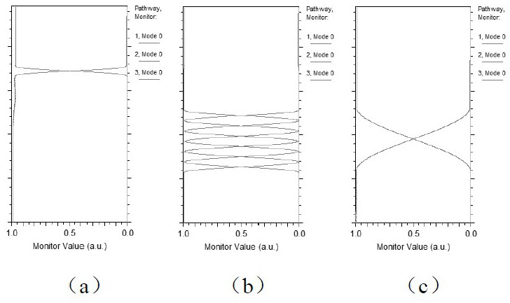
[0063] refer to Figure 4 As shown, the red, green, and blue monochromatic laser beams respectively enter the three optical waveguides through the coupler. The blue light has a wavelength of 450 nm, which is generated by a GaN-based semiconductor laser and enters the middle optical waveguide (in this embodiment, the lower The wavelength of green light is 520nm, which is generated by InAlGaN-based semiconductor laser, and enters the left optical waveguide (hereinafter referred to as optical waveguide 1 in this embodiment); the wavelength of red light is 638nm, which is produced by AlGaInP The base semiconductor las...

Embodiment 3

[0067] In order to increase the output power of red light, two red lasers, one green laser and one blue laser can be combined for light.

[0068] Schematic diagram of the optical waveguide section figure 1 As shown, there is a layer of SiO on a silicon wafer or glass substrate 2 The base layer has a thickness of 2 μm; the core layer of the optical waveguide is Si 3 N 4 , its thickness and width are both 0.16 μm; there is SiO on top 2 As a covering layer to ensure the reliability of the waveguide.

[0069] refer to Figure 5 As shown, the blue laser with a wavelength of 450 nm is coupled into the optical waveguide for propagating blue laser (left 1, referred to as optical waveguide 1 in this embodiment); the green laser with a wavelength of 520 nm is coupled into the optical waveguide for propagating green laser (left 2, referred to as optical waveguide 2 in this embodiment); red laser light with a wavelength of 638nm is coupled into the first optical waveguide for propaga...


PUM

PropertyMeasurementUnit
thicknessaaaaaaaaaa
thicknessaaaaaaaaaa
thicknessaaaaaaaaaa

Abstract

The invention discloses an optical waveguide type light combiner which comprises a plurality of optical waveguides for light incidence and a plurality of light wave coupling parts, and at most one section of light wave coupling part is arranged between any two optical waveguides for light incidence. The optical waveguide for light incidence includes a base layer, a core layer, and a cladding layer, and the relative refractive index difference between the core layer and the cladding layer is [Delta] 10%. When a plurality of beams of incident light are driven, the incident light forms a beam of emergent light after being coupled by the light wave coupling part, and the emergent light is emitted from the non-incident end of the optical waveguide for propagating the incident light with the non-longest wavelength. The invention further discloses a projection device adopting the optical waveguide type light combiner. Compared with the prior art, the optical waveguide type light combiner disclosed by the invention is high in light limiting capability, and the usable bending radius is smaller; a plurality of beams of light in different waveguides can be efficiently combined into one beam of waveguide; the overall coupling power loss of the light combiner is less than 25% of the incident light power.

Description

technical field [0001] The invention relates to an optical combiner, in particular to an optical waveguide type optical combiner and a projection device using the optical combiner, belonging to the technical field of optical projection display. Background technique [0002] In the prior art, there are display devices that take advantage of the good directivity of the laser and dynamically change the direction of the laser beam through scanning devices (galvanometers, scanning mirrors, etc.), so that images are projected onto the screen. In this display device, a monochromatic laser beam (usually a primary color laser beam) is combined as the light source of the display device, and the image display unit scans the transmitted light two-dimensionally and projects it into an image. [0003] This technology does not require complex optical components, the structure can be greatly simplified, and the light utilization efficiency is greatly increased. For the dark field in the sc...

Claims


Application Information

Patent Timeline
Patent Type & Authority Applications(China)
IPC IPC(8): G02B6/26G02B6/12G02B27/10G03B21/20
Inventor 司继成
Owner 苏州龙马璞芯芯片科技有限公司
Why Eureka
Try Eureka