Eureka AIR delivers breakthrough ideas for toughest innovation challenges, trusted by R&D personnel around the world.

Display substrate, preparation method thereof and display device

A display substrate and active layer technology, applied in the direction of electrical components, electrical solid devices, circuits, etc., can solve the problems of poor gray-scale transition of the display screen, poor anti-interference ability of stored screen data, and difficulty in effectively deploying low gray-scale, etc. Achieve the effects of simplifying the manufacturing process, eliminating the floating body effect, and avoiding adverse effects

Pending Publication Date: 2022-03-29
HEFEI VISIONOX TECH CO LTD
View PDF0 Cites 1 Cited by
  • Summary
  • Abstract
  • Description
  • Claims
  • Application Information

AI Technical Summary

Problems solved by technology

However, as an electronically conductive device, an oxide transistor has excellent switching performance, but when it is used as a driving transistor, it is easily limited by the extremely small sub-threshold swing (S.S. factor) or due to the range of voltage data of the driving chip. Due to the limitation of data range, it is difficult to effectively expand the middle and low grayscale or the anti-interference ability of the stored image data is poor, resulting in poor grayscale transition of the displayed image, which in turn affects the fineness and display uniformity of the displayed image

Method used


Image

  • Display substrate, preparation method thereof and display device
  • Display substrate, preparation method thereof and display device
  • Display substrate, preparation method thereof and display device

Examples


Embodiment Construction

[0063] In order to facilitate understanding of the present disclosure, the present disclosure will be described more fully below with reference to the related drawings. Preferred embodiments of the present disclosure are shown in the accompanying drawings. However, the present disclosure can be embodied in many different forms and is not limited to the embodiments described herein. On the contrary, these embodiments are provided to make the understanding of the disclosure of the present disclosure more thorough and comprehensive.

[0064] It should be understood that although the terms "first", "second", etc. may be used herein to describe various elements, they do not imply any order, quantity or importance, but are only used to distinguish different components. These terms are only used to distinguish one element from another. For example, a first element could be termed a second element, and, similarly, a second element could be termed a first element, without departing f...


PUM


Abstract

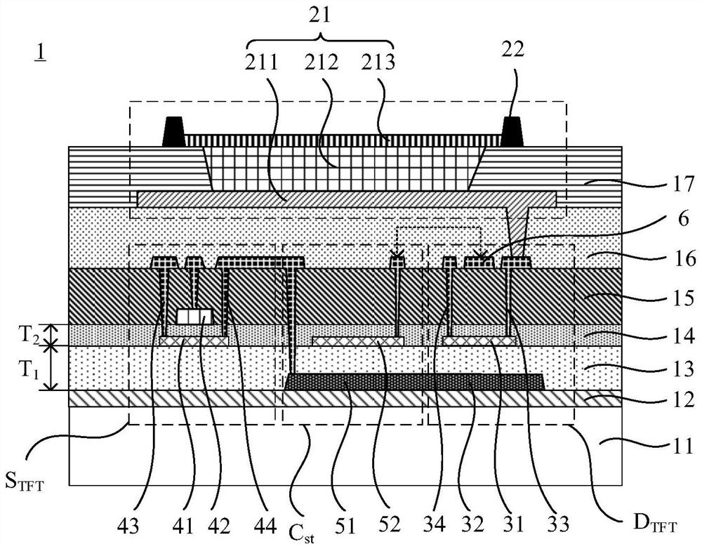
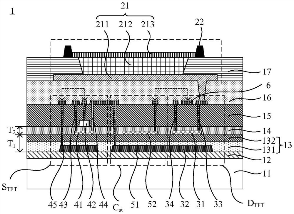
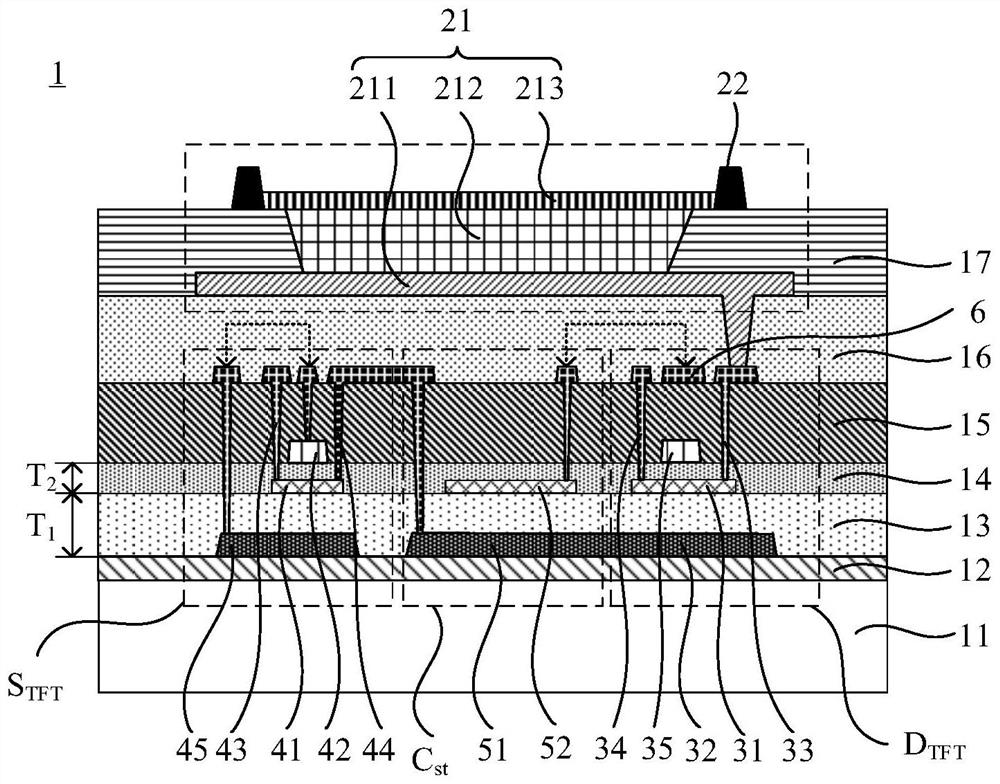
The invention relates to a display substrate, a preparation method thereof and a display device. The display substrate comprises a substrate and a plurality of driving circuits arranged on the substrate. The driving circuit includes a driving transistor and a switching transistor. The driving transistor comprises a first active layer and a first grid electrode located on the side, close to the substrate, of the first active layer. The switch transistor comprises a second active layer arranged on the same layer as the first active layer, and a second grid electrode located on the side, away from the substrate, of the second active layer. According to the display substrate, the preparation method thereof and the display device, the display performance of the display substrate can be improved, and the manufacturing process of the display substrate is simplified.

Description

technical field [0001] The present disclosure relates to the field of display technology, in particular to a display substrate, a manufacturing method thereof, and a display device. Background technique [0002] Active-matrix Organic Light Emitting Diode (AMOLED) display substrates are widely used in the display field due to their advantages of self-luminescence, high contrast ratio, and low power consumption. [0003] At present, the oxide (Oxide) backplane technology is used in the AMOLED display substrate, which has the advantages of simple manufacturing process, excellent device performance and good large-scale uniformity. However, as an electronically conductive device, an oxide transistor has excellent switching performance, but when it is used as a driving transistor, it is easily limited by the extremely small sub-threshold swing (S.S. factor) or due to the range of voltage data of the driving chip. Due to the limitation of data range, it is difficult to effectively...

Claims


Application Information

Patent Timeline
Patent Type & Authority Applications(China)
IPC IPC(8): H01L27/32
CPCH10K59/126H10K59/1213H10K59/12H10K59/1201
Inventor 王杰杜哲白青
Owner HEFEI VISIONOX TECH CO LTD
Why Eureka
Eureka Blog
Learn More