
MEMS pressure sensor and preparation method thereof

A pressure sensor, directly above the technology, applied in the field of micro-electromechanical system sensor design, can solve the problems of pressure measurement, linearity cannot be guaranteed, increase chip area, etc., achieve good sensitivity, save chip cost, and improve integration Effect

Pending Publication Date: 2022-03-25
SOUTHEAST UNIV
View PDF0 Cites 0 Cited by
  • Summary
  • Abstract
  • Description
  • Claims
  • Application Information

AI Technical Summary

Problems solved by technology

However, the thinner the strained membrane, the greater the deflection will be when it is subjected to external pressure. When the external pressure exceeds a certain threshold, the linearity will be lost. Therefore, it is not possible to measure the pressure under both low-pressure and high-pressure conditions.
At present, this type of pressure sensor can improve the sensitivity by forming a stress concentration area, and improve the linearity by local rigidity, but this method still cannot guarantee good linearity in a large measurement range; although it can also be set by setting Two different thickness strain films are used to make two pressure sensors for pressure measurement in a larger pressure range, but this method will increase the chip area, which is not conducive to the improvement of integration and the reduction of cost

Method used


Image

  • MEMS pressure sensor and preparation method thereof
  • MEMS pressure sensor and preparation method thereof
  • MEMS pressure sensor and preparation method thereof

Examples


Embodiment Construction

[0032] The present invention will be further explained below in conjunction with the accompanying drawings.

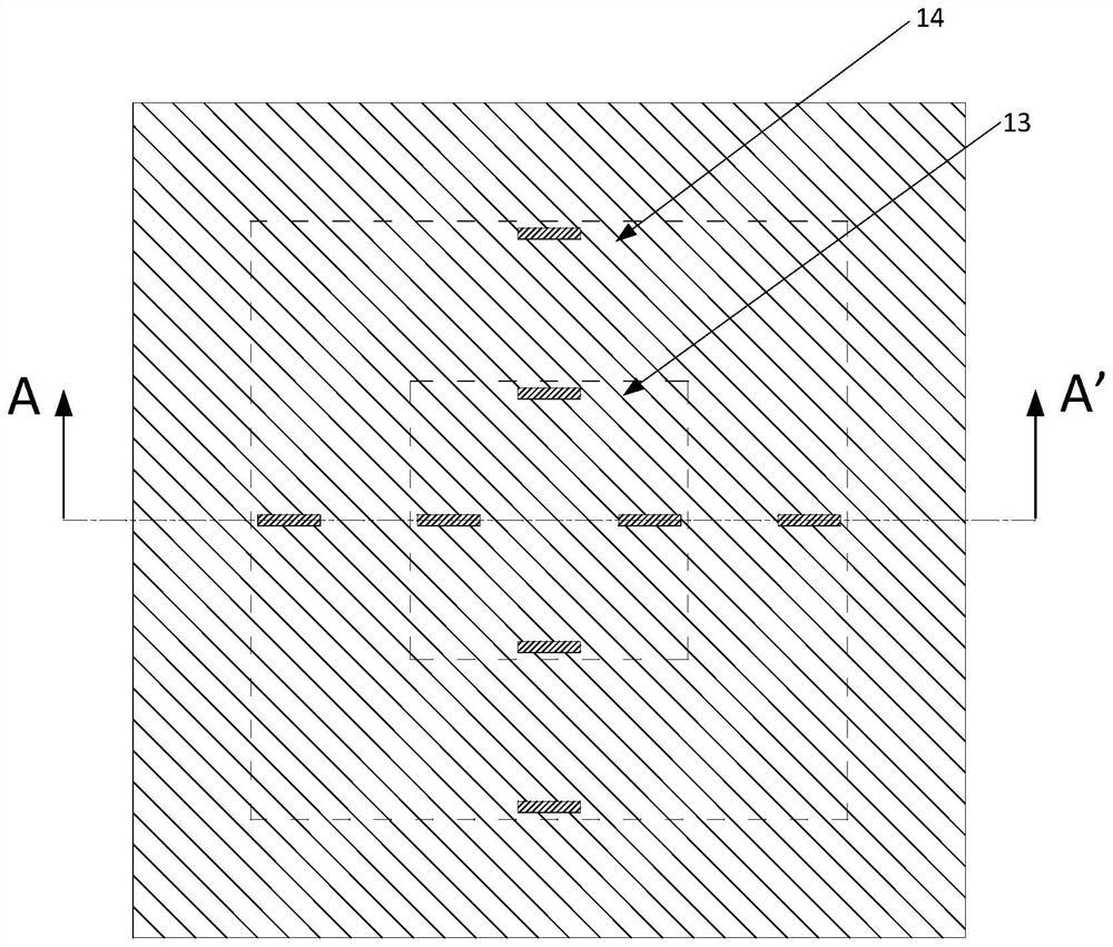
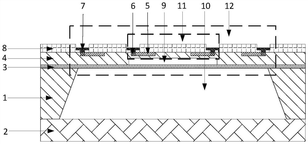
[0033] Such as figure 1 , figure 2 As shown, a MEMS pressure sensor includes a bulk silicon layer 1, a substrate 2, a buried oxide layer 3, a top silicon layer 4, a piezoresistor 5, an ohmic contact 6, a metal lead 7, an insulating dielectric layer 8, and a small cavity 9. Large cavity 10, thin strain film 11, thick strain film 12, inner Wheatstone bridge 13, outer Wheatstone bridge 14. The bulk silicon layer 1 is located on the upper surface of the substrate 2, the buried oxide layer 3 is located on the upper surface of the bulk silicon layer 1, the top silicon layer 4 is located on the upper surface of the buried oxide layer 3, and the piezoresistor 5 is located inside the top silicon layer 4, each A varistor 5 is separately provided with an ohmic contact 6 and is led out by a metal lead 7, wherein four varistors 5 form an inner Wheatstone bridge 13, and the other...


PUM

PropertyMeasurementUnit
thicknessaaaaaaaaaa
thicknessaaaaaaaaaa
thicknessaaaaaaaaaa

Abstract

The invention discloses an MEMS pressure sensor and a preparation method thereof. The MEMS pressure sensor comprises a bulk silicon layer, a substrate, a buried oxide layer, a top silicon layer, a piezoresistor, a stress film, an ohmic contact, a metal lead, an insulating dielectric layer, a small cavity, a large cavity, an inner Wheatstone bridge and an outer Wheatstone bridge. A small cavity is arranged in the top silicon layer, a large cavity is arranged in the bulk silicon layer, and the piezoresistor is arranged right above midpoints of four sides of the two cavities and in the top silicon layer. By arranging two Wheatstone bridges which are formed by two sets of piezoresistors and are located on stress films with different thicknesses, pressure in different measuring ranges is measured respectively, and the problems that a low-measuring-range pressure sensor loses linearity in a high-pressure environment and a high-measuring-range pressure sensor is low in sensitivity in a low-pressure environment are solved to a certain extent. The pressure sensor has a wide range and also has the sensitivity of a low-pressure environment; and meanwhile, the two cavities are stacked up and down in space, so that the chip area is saved, and the integration level is improved.

Description

technical field [0001] The invention belongs to the field of micro-electro-mechanical system (MEMS) sensor design, and relates to a MEMS pressure sensor and a method for manufacturing the pressure sensor by using a MEMS processing method. Background technique [0002] MEMS (Micro Electro Mechanical System) is a new interdisciplinary high-tech field. Its internal structure is generally on the order of microns or nanometers, and it is an independent intelligent system. The piezoresistive pressure sensor based on MEMS technology has the advantages of small size, easy integration, high reliability, and easy conversion of signals into electrical signals. It has been widely used in industrial control, biomedical, environmental monitoring, aerospace and other fields. Its working principle is that the thin film formed on the silicon wafer is made of varistors by ion implantation or diffusion to form a Wheatstone bridge. After the sensitive resistor is deformed, its resistance valu...

Claims


Application Information

Patent Timeline
Patent Type & Authority Applications(China)
IPC IPC(8): G01L1/18G01L9/06
CPCG01L1/18G01L9/06
Inventor 张志强王博廖俊杰黄晓东
Owner SOUTHEAST UNIV
Learn More