Optical waveguide assembly and display device including the same
A technology of optical waveguide and components, which is applied in the field of optical transmission, can solve the problems of large overall thickness of display equipment, unfavorable miniaturization and light weight of equipment, and achieve the effects of simple structure, easy manufacturing, and simple control method
- Summary
- Abstract
- Description
- Claims
- Application Information
AI Technical Summary
Problems solved by technology
Method used
Image
Examples
Embodiment 1
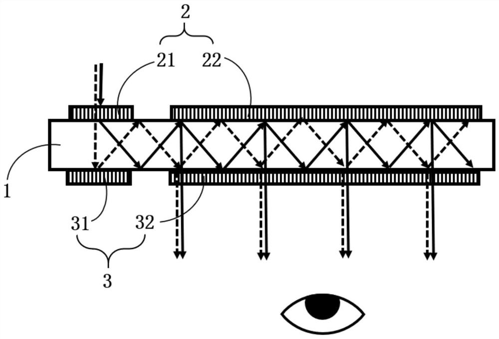
[0061] figure 1 A schematic structural diagram of an optical waveguide assembly provided by an embodiment of the present application.
[0062] Such as figure 1 As shown, this embodiment provides an optical waveguide assembly, including:
[0063] The waveguide 1 includes a first optical surface and a second optical surface opposite to the first optical surface, and the waveguide 1 is used for total reflection and transmission of light therein; and
[0064] At least two diffractive units, where
[0065] - the first diffraction unit 2, comprising a first in-coupling liquid crystal grating 21 and a first out-coupling liquid crystal grating 22 arranged on the first optical surface, the first in-coupling liquid crystal grating 21 and the first out-coupling liquid crystal grating 22 are set to When the voltage or no voltage is applied, it is in the grating state in the first direction, and the first coupling-in liquid crystal grating 21 is used to couple the first light into the w...
Embodiment 2
[0114]The optical waveguide assembly provided in this embodiment also includes a third diffraction unit (not shown in the figure), the third diffraction unit includes a third in-coupling liquid crystal grating and a third out-coupling liquid crystal grating, the third in-coupling liquid crystal grating is arranged on the first An in-coupling liquid crystal grating 21 is arranged on a surface opposite to the waveguide plate 1 or a second in-coupling liquid crystal grating 31 is arranged on a surface opposite to the waveguide plate 1, and a third out-coupling liquid crystal grating is arranged on the first out-coupling liquid crystal grating The grating 22 is arranged on a surface opposite to the waveguide plate 1 or on a surface of the second outcoupling liquid crystal grating 32 opposite to the waveguide plate 1, and the third incoupling liquid crystal grating and the third outcoupling liquid crystal grating are arranged to be The raster state in the first direction when voltag...
Embodiment 3
[0125] Figure 5 It is a schematic structural diagram of a display device provided by an embodiment of the present application.
[0126] Such as Figure 5 As shown, this embodiment also provides a display device, including:
[0127] The projection light machine 10, the projection light machine 10 includes a display chip 101 and a projection lens 102, the display chip 101 is used to control the output of the first light and the second light of the display image at a certain frequency in time sequence, and the projection lens 102 is used to project the display chip 101 output light; and
[0128] The optical waveguide assembly, the optical waveguide assembly is the optical waveguide assembly described in any of the above embodiments, at least the first coupling liquid crystal grating 21 of the first diffraction unit 2 of the optical waveguide assembly and the second coupling liquid crystal grating 21 of the second diffraction unit 3 The grating 31 is used to couple the light p...
PUM
| Property | Measurement | Unit |
|---|---|---|
| thickness | aaaaa | aaaaa |
| thickness | aaaaa | aaaaa |
| refractive index | aaaaa | aaaaa |
Abstract
Description
Claims
Application Information
 - R&D Engineer
- R&D Manager
- IP Professional
- Industry Leading Data Capabilities
- Powerful AI technology
- Patent DNA Extraction
Browse by: Latest US Patents, China's latest patents, Technical Efficacy Thesaurus, Application Domain, Technology Topic, Popular Technical Reports.
© 2024 PatSnap. All rights reserved.Legal|Privacy policy|Modern Slavery Act Transparency Statement|Sitemap|About US| Contact US: help@patsnap.com


