Inorganic electroluminescent display and its manufacturing method

A luminescent and display technology, which is applied in the direction of circuits, electrical components, semiconductor devices, etc., can solve the problems of reducing the withstand voltage performance of devices, low dielectric constant of the dielectric layer, and increased leakage, so as to reduce the requirements of the environment and equipment, and improve Brightness and overall efficiency, effects of reducing leakage and dielectric loss

Inactive Publication Date: 2006-07-26
INESA ELECTRON
View PDF0 Cites 2 Cited by
  • Summary
  • Abstract
  • Description
  • Claims
  • Application Information

AI Technical Summary

Problems solved by technology

[0004] 1) The thickness of the upper dielectric layer 25 and the lower dielectric layer 23 are basically the same. In the specific manufacturing process, since the light-emitting layer has to undergo a high-temperature annealing process, the lower dielectric layer must also be annealed at the same time, resulting in a greatly reduced pressure resistance of the lower dielectric layer. , The leakage increases again, thereby reducing the withstand voltage performance of the entire device and increasing the leakage of the entire device, which affects the brightness and life of the device, and increases the power consumption of the device;
[0005] 2) Since the thickness of the lower dielectric layer 23 is too thick, a considerable part of the visible light emitted from the light-emitting layer is absorbed by the lower dielectric layer 23, and a part is reflected and refracted, which reduces the brightness and overall efficiency of the device;
[0006] 3) The upper dielectric layer 25 and the lower dielectric layer 23 in the traditional electroluminescent display are made of materials with low dielectric constants such as tantalum pentoxide, yttrium trioxide, aluminum oxide, samarium trioxide, silicon nitride, etc. material, such shortcomings are also obvious: on the one hand, there are not enough electrons with a certain well depth on the interface state between the light-emitting layer and the dielectric layer; on the other hand, due to the low dielectric constant of the dielectric layer, in order to maintain a lower threshold voltage, The thickness of the dielectric layer is generally thin (300-500 nanometers), and such a thin film has higher requirements on the environment during the preparation process, which increases the production cost and reduces the yield; and these dielectric materials cannot be applied to high Inorganic electroluminescent display devices with dielectric constant and high avalanche threshold field strength luminescent materials have significant limitations

Method used


Image

  • Inorganic electroluminescent display and its manufacturing method
  • Inorganic electroluminescent display and its manufacturing method
  • Inorganic electroluminescent display and its manufacturing method

Examples


Embodiment 1

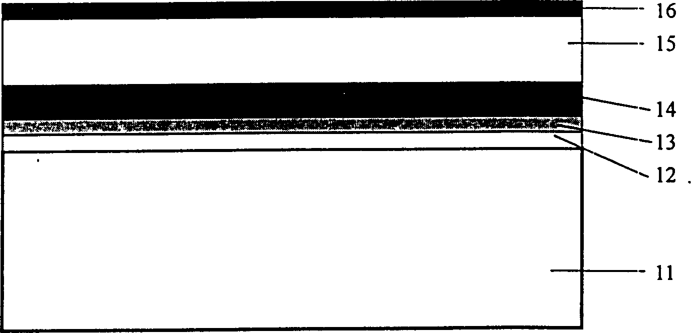
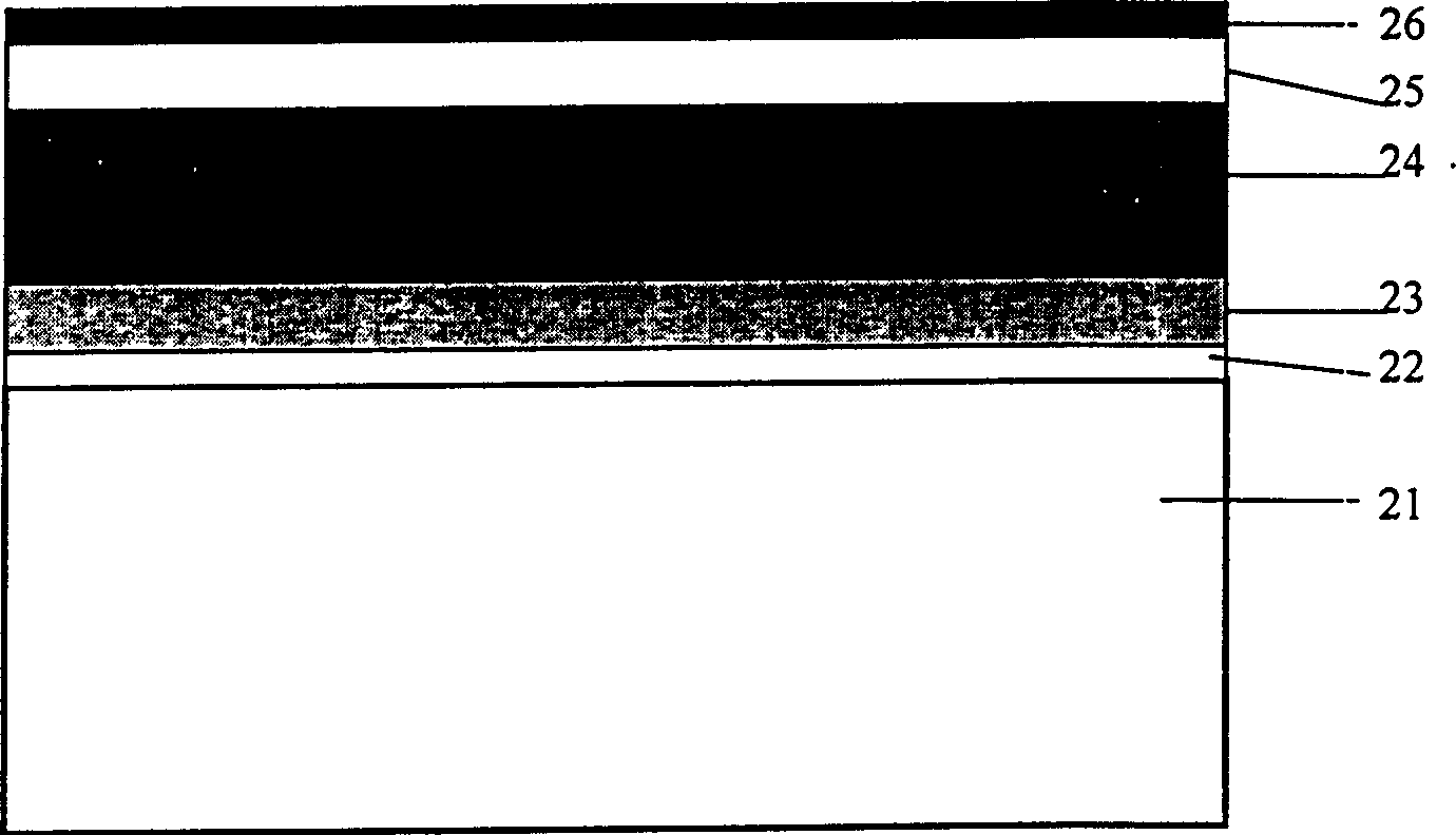
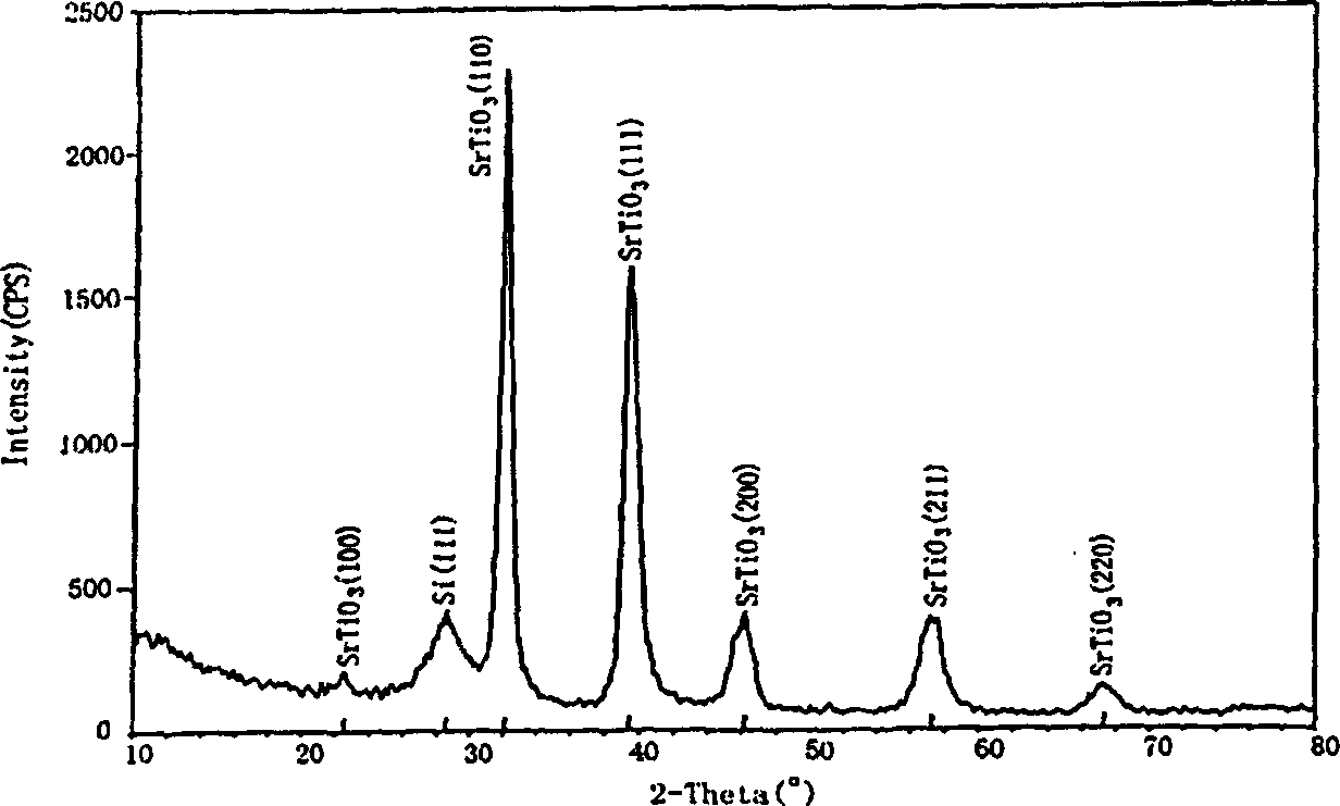
[0073] Embodiment 1. The lower electrode adopts a 150nm thick ITO electrode, the lower dielectric layer adopts 100nm strontium titanate, the light-emitting layer adopts 600nm manganese-doped zinc sulfide, and the upper dielectric layer adopts a composite of 300nm strontium titanate and 300nm tantalum pentoxide film, and the upper electrode is a 150nm aluminum electrode deposited by sputtering. The sputtering condition of the lower dielectric layer strontium titanate: the background vacuum is 4.0×10 -3 Pa, Ar / O 2 The ratio is 4:1, the sputtering pressure is 1.7 Pa, the substrate temperature is 500° C., the target base distance is 5 cm, the sputtering power is 400 W, and the sputtering time is 10 minutes. The light-emitting layer ZnS:Mn is deposited by electron beam evaporation, the substrate temperature is 173°C, and the background vacuum is 3.7×10 -3 Pa. The sputtering process of the strontium titanate layer in the upper dielectric layer is: the background vacuum is 1.4×10 ...

Embodiment 2

[0074] Embodiment 2, the lower electrode adopts a 150nm thick ITO electrode, the lower dielectric layer adopts 200nm strontium titanate, the light-emitting layer adopts 600nm manganese-doped zinc sulfide, and the upper dielectric layer adopts a composite of 200nm strontium titanate and 400nm tantalum pentoxide film, the upper electrode is a 150nm aluminum electrode. The sputtering condition of the lower dielectric layer strontium titanate: the background vacuum is 8.3×10 -4 Pa, Ar / O 2 The ratio is 4:1, the sputtering pressure is 1.3 Pa, the substrate temperature is 530° C., the target base distance is 5 cm, the sputtering power is 400 W, and the sputtering time is 9 minutes. The light-emitting layer ZnS:Mn is deposited by electron beam evaporation, the substrate temperature is 165°C, and the background vacuum is 2.6×10 -3 Pa. The sputtering condition of strontium titanate in the upper dielectric layer is: the background vacuum is 8.3×10 -3 Pa, Ar / O 2 The ratio is 3:2, the...

Embodiment 3

[0075] Embodiment 3. The lower electrode is made of 150nm thick ITO electrode, the lower dielectric layer is made of 200nm strontium titanate, the light-emitting layer is made of 600nm manganese-doped zinc sulfide, and the upper dielectric layer is made of 200nm strontium titanate and 500nm tantalum pentoxide. film, and the upper electrode is a 150nm aluminum electrode deposited by sputtering. The sputtering condition of the lower dielectric layer strontium titanate: the background vacuum is 8.4×10 -4 Pa, Ar / O 2 The ratio is 4:1, the sputtering pressure is 1.3 Pa, the substrate temperature is 550° C., the target base distance is 5 cm, the sputtering power is 400 W, and the sputtering time is 20 minutes. The light-emitting layer ZnS:Mn is deposited by electron beam evaporation, the substrate temperature is 165°C, and the background vacuum is 1.8×10 -3 Pa. Before sputtering the upper dielectric layer of strontium titanate, the sample was annealed in the sputtering chamber at ...


PUM


Abstract

This invention discloses one inorganic electroluminescence display and its process method and relates to the relative technique field suitable for alternating driving, wherein, the display upper dielectric layer is thicker than the down one; the dielectric layer touching to the light layer adopts high dielectric parameter materials; the light layer is mixed with light semiconductor layer; the said upper dielectric layer is formed by multiple compound medium film. The invention method processes some parts by annealing procedure to omit one light layer annealing process.

Description

technical field [0001] The invention belongs to the technical field of flat panel display, in particular to an inorganic electroluminescent display suitable for AC driving. Background technique [0002] Inorganic electroluminescent flat-panel displays have the characteristics of all solid state, light weight, thin thickness, large viewing angle, and simple structure. They can be used in harsh environments such as low temperature and vibration, and can realize large-area color dynamic display. They have a wide range of applications. prospect. Traditional inorganic electroluminescent displays generally use a low dielectric constant dielectric layer (dielectric constant lower than 50), and the upper and lower dielectric layers are symmetrically distributed on both sides of the light-emitting layer. The device is prone to breakdown due to dust pollution. The structure of the traditional electroluminescent display is as follows figure 2 As shown, it is composed of glass 21 , tr...

Claims


Application Information

Patent Timeline
Patent Type & Authority Applications(China)
IPC IPC(8): H01L33/00
Inventor 肖田刘逸忠徐毅林明通楼均辉
Owner INESA ELECTRON
Why Eureka
Try Eureka