Circuit board and hole forming method thereof

A circuit board and hole technology, which is applied to the formation of electrical connections of printed components, printed circuits, printed circuits, etc., can solve the problems of reduced reliability of circuit boards, limited capacity of conductive materials, cracks, etc., to reduce the probability of cracks and improve reliability. degree of effect

Pending Publication Date: 2022-02-22
UNIMICRON TECH CORP
View PDF0 Cites 0 Cited by
  • Summary
  • Abstract
  • Description
  • Claims
  • Application Information

AI Technical Summary

Problems solved by technology

[0003] The shape of a general hole (such as a blind hole or a solder mask opening), that is, the shape of the inner space of the hole, is basically a frustum, so most of the above-mentioned holes have a relatively flat hole wall, so that the insulating layer fixes the conductive material in the hole. Materials (such as conductive pillars or solder) have limited capabilities, which may cause cracks to separate from the conductive material and the underlying pads, resulting in reduced reliability of the circuit board

Method used


Image

  • Circuit board and hole forming method thereof
  • Circuit board and hole forming method thereof
  • Circuit board and hole forming method thereof

Examples


Embodiment Construction

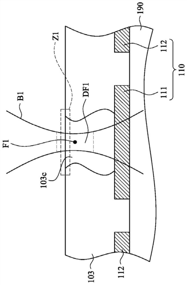
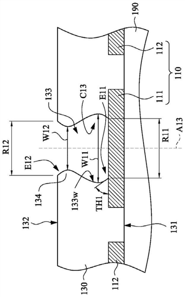
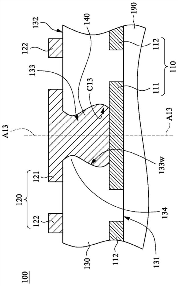
[0044] In the following text, in order to clearly present the technical features of this application, the dimensions (such as length, width, thickness, and depth) of elements (such as layers, films, substrates, and regions) in the drawings will be enlarged in a non-proportional manner . Therefore, the description and explanation of the following embodiments are not limited to the size and shape of the elements in the drawings, but should cover the deviations in size, shape and both caused by actual manufacturing process and / or tolerances. For example, a planar surface shown in the drawings may have rough and / or non-linear features, while acute angles shown in the drawings may be rounded. Therefore, the components shown in the drawings of this case are mainly for illustration, and are not intended to accurately depict the actual shape of the components, nor are they used to limit the scope of the patent application of this case.

[0045] Secondly, words such as "about", "appro...


PUM


Abstract

The invention relates to a circuit board and a hole forming method thereof. The circuit board comprises a photosensitive insulating layer and a first circuit layer. The photosensitive insulating layer has a hole, and a first surface and a second surface opposite to each other. The hole is provided with a first port formed on the first surface, a second port formed on the second surface, an axis and a hole wall surrounding the axis. Part of the hole wall extends towards the axis to form at least one annular flange. The first circuit layer is arranged on the first surface and comprises a first connecting pad, and the first connecting pad is exposed by the hole. At least one concave cavity is formed between the annular flange and the first connecting pad. The minimum width of the annular flange is smaller than the maximum width of the concave cavity.

Description

technical field [0001] The invention relates to a circuit board and a method for forming holes thereof. Background technique [0002] The insulating layer of existing circuit boards (such as solder mask or dielectric layer in the board) will have one or more holes, such as blind holes or solder mask openings, and these holes will usually be filled with conductive materials, where the conductive The material is connected to pads on the circuit layer. For example, the blind holes in the dielectric layer in general circuit boards are usually filled with conductive posts, and the solder resist openings in the solder resist layer are usually filled with solder, wherein the conductive posts and the solder are both Connect to the underlying pads to electrically connect the circuit layer. [0003] The shape of a general hole (such as a blind hole or a solder mask opening), that is, the shape of the inner space of the hole, is basically a frustum, so most of the above-mentioned hol...

Claims


Application Information

Patent Timeline
IPC IPC(8): H05K1/11H05K3/00H05K3/42
CPCH05K1/116H05K3/0023H05K3/42H05K3/423H05K2201/09563
Inventor 杨凯铭林晨浩林伯诚
Owner UNIMICRON TECH CORP
Why Eureka
Try Eureka