Diode packaging structure and packaging process thereof

A technology of packaging structure and packaging technology, which is applied in the direction of electrical components, electric solid devices, circuits, etc., can solve problems such as hidden dangers of chip quality and large stress changes in diode packaging structures, and achieve large stress changes, good conduction and heat dissipation effects, and convenience The effect of encapsulation

Pending Publication Date: 2022-02-11
江苏固得沃克微电子科技有限公司
View PDF0 Cites 0 Cited by
  • Summary
  • Abstract
  • Description
  • Claims
  • Application Information

AI Technical Summary

Problems solved by technology

[0006] The invention provides a diode packaging structure and its packaging process, which solves the problem that the diode packaging structure has a large stress change before and after welding, which leads to potential hidden quality problems when the chip is used

Method used


Image

  • Diode packaging structure and packaging process thereof
  • Diode packaging structure and packaging process thereof
  • Diode packaging structure and packaging process thereof

Examples


Embodiment Construction

[0031] The present invention will be further described below in conjunction with the accompanying drawings and embodiments.

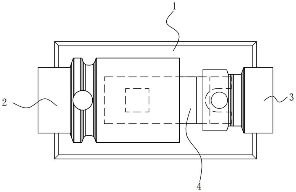
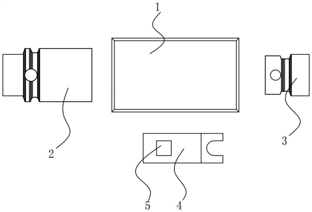
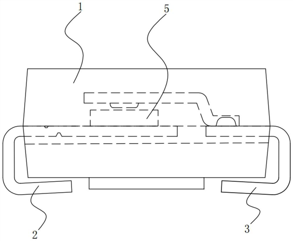
[0032] Please refer to figure 1 , figure 2 , image 3 , Figure 4 and Figure 5 ,in, figure 1 A structural schematic diagram of a preferred embodiment of the diode packaging structure and its packaging process provided by the present invention; figure 2 for figure 1 The disassembly schematic diagram; image 3 for figure 2 The schematic diagram of the internal structure of the front view part of the package shown; Figure 4 for figure 2 The side view of the plastic package shown; Figure 5 A flow chart of the diode packaging process provided by the present invention. The diode packaging structure and its packaging process include: a plastic package 1;

[0033] A first tablet 2, the first tablet 2 is arranged on one side of the plastic package;

[0034] The second sheet 3, the second sheet 3 is arranged on one side of the plastic package;...


PUM


Abstract

The invention provides a diode packaging structure and a packaging process thereof. The diode packaging structure comprises a plastic packaging body, a first material piece, a second material piece, a jumper wire and a chip; the first material piece is arranged on one side of the plastic package body; the second material piece is arranged on one side of the plastic package body; the jumper wire is arranged between the first material piece and the second material piece; and the chip is arranged between the first material piece and the jumper wire. According to the diode packaging structure and the packaging process thereof, the Clip process is adopted to form a monolithic matrix type material piece structure, the chip is in lap joint with the other pin of the first material piece through the Clip to form a whole, the Clip is naturally attached to the chip and the first material piece due to the gravity of the Clip, the stress influence before and after welding is very small, and due to the fact that the usage amount of copper and soldering tin is large, the packaging of the diode is more convenient, and the disadvantage that the stress change is large before and after the matrix type material piece diode is packaged is greatly improved.

Description

technical field [0001] The invention relates to the technical field of diode packaging, in particular to a diode packaging structure and a packaging process thereof. Background technique [0002] Diode is one of the earliest semiconductor devices, and its application is very extensive, especially in various electronic circuits, using diodes and components such as resistors, capacitors, and inductors to make reasonable connections to form circuits with different functions, which can realize AC current It has various functions such as rectification, detection of modulated signals, limiting and clamping, and voltage stabilization of power supply voltage. [0003] When the diode is used, it is often necessary to package the diode. The diode package refers to connecting the circuit pins on the silicon chip to the external joints with wires so as to connect with other devices. [0004] In the prior art, the diodes are usually packaged using a double-chip process, that is, two mat...

Claims


Application Information

Patent Timeline
Patent Type & Authority Applications(China)
IPC IPC(8): H01L23/49H01L23/488H01L21/48H01L21/60
CPCH01L23/49H01L23/488H01L21/4885H01L21/4871H01L24/85H01L24/84H01L2224/85H01L2224/84
Inventor 苏荻楠
Owner 江苏固得沃克微电子科技有限公司
Why Eureka
Try Eureka