
Chip on film, GOA driving method and display device

A technology of chip-on-chip film and driving method, which is applied in the field of GOA driving method and display device, and chip-on-chip film, which can solve the problems of small COF bonding pin area, limited number of conductive particles, and missing Ni coating, so as to avoid defects, reduce metal corrosion, The effect of optimizing layout

Active Publication Date: 2022-02-08
BOE TECH GRP CO LTD +1
View PDF9 Cites 0 Cited by
  • Summary
  • Abstract
  • Description
  • Claims
  • Application Information

AI Technical Summary

Problems solved by technology

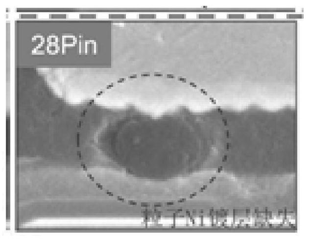
[0003] However, when the driving voltage increases, the metal Ni ions in the ACF conductive adhesive in the Bonding pin where the COF Bonding position is at a high potential are prone to electrochemical corrosion in a high-temperature and high-humidity (85°C, 85% R.H.) environment Ni-2e=Ni ^2+, resulting in the lack of Ni plating. Due to the small area of ​​the COF bonding pin, the commonly used pin width is 12um, the gap is 18um, and the length is only 0.4mm. The number of conductive particles is limited, and the product will fail under long-term action.

Method used


Image

  • Chip on film, GOA driving method and display device
  • Chip on film, GOA driving method and display device
  • Chip on film, GOA driving method and display device

Examples


Embodiment Construction

[0039] The application will be further described in detail below in conjunction with the accompanying drawings and embodiments. It should be understood that the specific embodiments described here are only used to explain related inventions, rather than to limit the invention. It should also be noted that, for ease of description, only parts related to the invention are shown in the drawings.

[0040] It should be noted that, in the case of no conflict, the embodiments in the present application and the features in the embodiments can be combined with each other. The present application will be described in detail below with reference to the accompanying drawings and embodiments.

[0041] The display panel needs to be bonded during preparation, which is mainly to connect the panel with COF (chip-on-chip film) and FPC (flexible circuit board) through gold fingers, so that the panel has functions such as power supply, display, and touch. In COF (chip on film) technology, the d...


PUM


Abstract

The invention discloses a chip on film, a GOA driving method and a display device. The chip on film comprises a plurality of pins arranged in an array, wherein the pins comprise signal terminals and redundant terminals; a plurality of adjacent pins form a first pin area; the signal terminals in the first pin area are double-pin signals; the adjacent pins in the double-pin signals correspond to the same signal; and the redundant terminals are arranged on two sides of the first pin area. According to the chip on film provided by the embodiment of the invention, by optimizing an arrangement mode of the pins, metal corrosion of a binding area is reduced, voltage differences between the pins are reduced, and duration of high voltage differences is shortened; a time sequence of driving signals is optimized, so that the optimization effect is further improved, and badness caused by the metal corrosion is avoided; and under the condition that a charging rate is not influenced, the problem of abnormal display of a high-frequency product under high-temperature and high-humidity reliability is solved, and the reliability of the product is improved.

Description

technical field [0001] The present application generally relates to the field of display technology, and specifically relates to a chip-on-chip film, a GOA driving method, and a display device. Background technique [0002] In recent years, in order to pursue more stable images, smoother dynamic image performance, and better gaming experience of display products, the market share of high refresh rate mobile phone products has gradually increased. However, a high frame rate means that the display time of each frame is reduced. When the resolution remains unchanged, the charging time of the pixel is reduced accordingly. When the frame rate is high, there may be a problem of insufficient charging time. In order to solve the problem of insufficient charging of the pixel, the driving voltage of the product will be increased to speed up the charging speed of the pixel. [0003] However, when the driving voltage increases, the metal Ni ions in the ACF conductive adhesive in the Bo...

Claims


Application Information

Patent Timeline
IPC IPC(8): G09G3/36G09G3/3208
CPCG09G3/36G09G3/3208
Inventor 田婷石爽许梦兴王珍杜育锋舒兴军杨胜伟高宗丽安娜杨瑞锋李志
Owner BOE TECH GRP CO LTD
Learn More