
High-efficiency fixing device for semiconductor material four-probe measuring instrument

A fixed device and semiconductor technology, which is applied to measuring devices, measuring device casings, instruments, etc., can solve the problems of low detection efficiency, easily crushed materials, irregular surfaces, etc., and achieves the effect of high intelligence and high detection efficiency.

Inactive Publication Date: 2022-01-04
邱大滨
View PDF0 Cites 0 Cited by
  • Summary
  • Abstract
  • Description
  • Claims
  • Application Information

AI Technical Summary

Problems solved by technology

[0002] New electronic materials refer to a class of materials with functional properties such as energy and signal emission, absorption, conversion, transmission, storage, display or processing, including conductive materials, semiconductor materials, magnetic materials, optoelectronic materials, new energy materials, etc., among which A type of electronic material whose electrical conductivity is between that of a conductor and an insulator, and whose electrical conductivity changes significantly with changes in the environment. The use of semiconductor materials requires a four-probe tester to test the resistivity and sheet resistance. The existing The fixing device of the four-probe tester can only fix a single semiconductor material. After the test is completed, the material needs to be removed and then another material is fixed. The detection efficiency is low. At the same time, some materials are small and have irregular surfaces, which are difficult and easy to fix. Crush the material, resulting in material waste
[0003] Aiming at the deficiencies of the prior art, the present invention provides a high-efficiency semiconductor material four-probe tester fixing device, which can automatically fix and take out the material, has high detection efficiency, and can be applied to materials of different shapes and sizes. The advantages of adjusting the clamping force of the material and high degree of intelligence solve the problem that the existing four-probe tester's fixing device can only fix a single semiconductor material. After the test is completed, the material needs to be removed, and then another material is fixed, which improves the detection efficiency. Low, at the same time, some materials are small and irregular in surface, difficult to fix, and easy to crush the material, resulting in material waste

Method used


Image

  • High-efficiency fixing device for semiconductor material four-probe measuring instrument
  • High-efficiency fixing device for semiconductor material four-probe measuring instrument
  • High-efficiency fixing device for semiconductor material four-probe measuring instrument

Examples


Embodiment 1

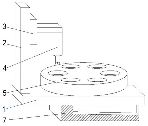
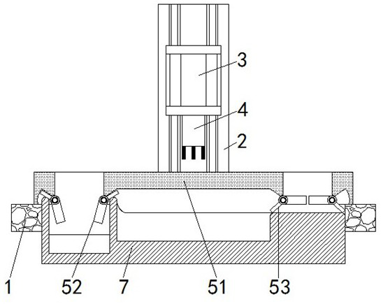
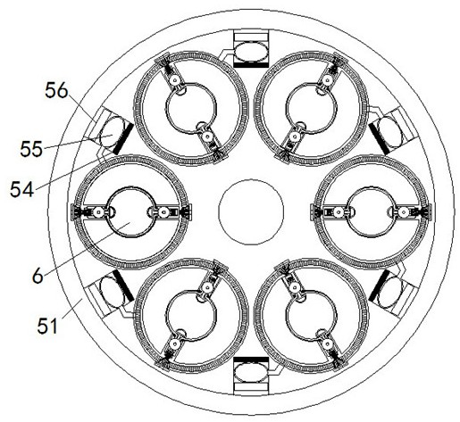
[0024] see Figure 1-3 , a high-efficiency semiconductor material four-probe tester fixture, including a base 1, the top of the base 1 is equipped with a positioning mechanism 5, the positioning mechanism 5 includes a positioning plate 51, the bottom of the positioning plate 51 is hinged with a base plate 52, the base plate The inside of 52 is fixedly connected with spring, and base plate 52 is evenly distributed on the bottom of positioning plate 51, and base plate 52 is corresponding to fixing mechanism 6, and the outside of base plate 52 is fixedly connected with pressure bar 53, and the inside of positioning plate 51 is fixedly connected with Electromagnet 54, the outer side of electromagnet 54 is fixedly connected with regulating capsule 55, and the side of regulating capsule 55 away from electromagnet 54 is fixedly connected with sucking plate 56, according to the characteristic of material, regulates the electric current that electromagnet 54 passes, and electromagnet 54...

Embodiment 2

[0026] see Figure 1-5 A high-efficiency semiconductor material four-probe tester fixing device includes a base 1 and a slide rail 2, the slide rail 2 is welded on the top of the base 1, the front of the slide rail 2 is slidably connected with a slider 3, the slide The front of the block 3 is fixedly connected with a detector 4, the top of the base 1 is fixedly connected with a positioning mechanism 5, and the inside of the positioning mechanism 5 is fixedly connected with a fixing mechanism 6. The fixing mechanism 6 includes a fixing frame 61, and the fixing frame 61 is inserted into the positioning mechanism. 5, the inside of the fixed frame 61 is fixedly connected with a runner 62, the top of the runner 62 is engaged with a transmission wheel 63, and the side of the transmission wheel 63 near the axis of the fixed frame 61 is fixedly connected with a screw 64, and the inside of the fixed frame 61 A slide bar 65 is slidably connected, and the bottom of the slide bar 65 is fi...

Embodiment 3

[0028] see Figure 1-5A high-efficiency semiconductor material four-probe tester fixing device includes a base 1 and a slide rail 2, the slide rail 2 is welded on the top of the base 1, the front of the slide rail 2 is slidably connected with a slider 3, the slide The front of block 3 is fixedly connected with detector 4, and the top of base 1 is fixedly connected with positioning mechanism 5, and positioning mechanism 5 comprises positioning disc 51, and the bottom of positioning disc 51 is hinged with base plate 52, and the inside of base plate 52 is fixedly connected with spring, And the base plate 52 is evenly distributed on the bottom of the positioning disc 51, and the base plate 52 corresponds to the fixing mechanism 6, the outside of the base plate 52 is fixedly connected with a pressure bar 53, the inside of the positioning disc 51 is fixedly connected with an electromagnet 54, and the outside of the electromagnet 54 An adjustment bag 55 is fixedly connected, and the ...


PUM


Abstract

The invention provides a high-efficiency fixing device for a semiconductor material four-probe measuring instrument, and relates to the technical field of new electronic materials. The high-efficiency fixing device for the semiconductor material four-probe measuring instrument comprises a base, a positioning mechanism is installed at the top of the base, the positioning mechanism comprises a positioning disc, and a suction plate is fixedly connected to the side, away from an electromagnet, of an adjusting bag. According to the high-efficiency fixing device for the semiconductor material four-probe measuring instrument, the electromagnet is electrified to generate magnetic force to drive the suction plate to slide, the suction plate extrudes the adjusting bag, the adjusting bag enables air pressure in a top bag to be increased through an air pipe, thrust of the top bag to an air valve is increased, and the air valve enables clamping force of an ejector block to be increased; the current of the electromagnet is controlled, therefore, the magnetic force of the electromagnet is controlled, and the clamping force is controlled; and through cooperative use of the ejector block and a stop switch, the effects that the clamping force can be adjusted according to materials, and the intelligent degree is high are achieved.

Description

technical field [0001] The invention relates to the technical field of new electronic materials, in particular to a high-efficiency fixing device for a four-probe tester for semiconductor materials. Background technique [0002] New electronic materials refer to a class of materials with functional properties such as energy and signal emission, absorption, conversion, transmission, storage, display or processing, including conductive materials, semiconductor materials, magnetic materials, optoelectronic materials, new energy materials, etc., among which A type of electronic material whose electrical conductivity is between that of a conductor and an insulator, and whose electrical conductivity changes significantly with changes in the environment. The use of semiconductor materials requires a four-probe tester to test the resistivity and sheet resistance. The existing The fixing device of the four-probe tester can only fix a single semiconductor material. After the test is c...

Claims


Application Information

Patent Timeline
Patent Type & Authority Applications(China)
IPC IPC(8): G01R1/04
CPCG01R1/0425
Inventor 邱大滨
Owner 邱大滨
Learn More