
Bi-HEMT device and preparation method thereof

A device and area technology, applied in the field of Bi-HEMT devices and their preparation, can solve problems such as large leakage current, complicated device structure design, and increased device power consumption, so as to increase device power consumption, avoid device power consumption, and solve The effect of larger leakage current

Pending Publication Date: 2021-12-24
泉州市三安集成电路有限公司
View PDF0 Cites 0 Cited by
  • Summary
  • Abstract
  • Description
  • Claims
  • Application Information

AI Technical Summary

Problems solved by technology

Because the pHEMT it uses is an N-channel device, this will cause a large leakage current in the device. In order to avoid excessive leakage current, the more commonly used method is to design an additional impedance structure on the BiHEMT device to reduce the leakage current. , which complicates the structural design of the entire device and increases the power consumption of the device

Method used


Image

  • Bi-HEMT device and preparation method thereof
  • Bi-HEMT device and preparation method thereof
  • Bi-HEMT device and preparation method thereof

Examples


Embodiment Construction

[0031] The embodiments set forth below represent the information necessary to enable one skilled in the art to practice the embodiments and illustrate the best mode of practicing the embodiments. Upon reading the following description with reference to the accompanying drawing figures, those skilled in the art will understand the concepts of the invention and will recognize applications of these concepts not particularly addressed herein. It should be understood that these concepts and applications are within the scope of the invention and the appended claims.

[0032]It will be understood that, although the terms first, second, etc. may be used herein to describe various elements, these elements should not be limited by these terms. These terms are only used to distinguish one element from another. For example, a first element could be termed a second element, and, similarly, a second element could be termed a first element, without departing from the scope of the present in...


PUM


Abstract

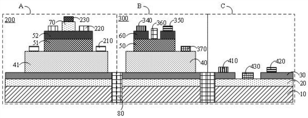
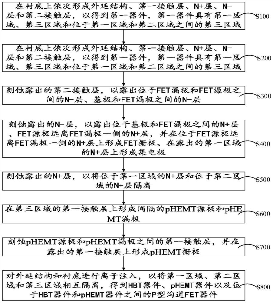
The invention discloses a Bi-HEMT device and a preparation method thereof, and relates to the technical field of semiconductors. The Bi-HEMT device comprises a substrate, an HBT device, a P-type channel FET device and a pHEMT device, wherein the substrate is provided with a first region, a second region and a third region, the HBT device is formed on the first region, the P-type channel FET device is formed on the second region, and the pHEMT device is formed on the third region, wherein the first region, the second region and the third region are arranged in a pairwise isolation mode, and the P-type channel FET device is located between the HBT device and the pHEMT device. According to the Bi-HEMT device, the leakage current of the device can be reduced.

Description

technical field [0001] The invention relates to the technical field of semiconductors, in particular to a Bi-HEMT device and a preparation method thereof. Background technique [0002] Compared with silicon-based field effect transistors, heterojunction bipolar transistors (HBTs) have better power handling capabilities and linearity, and are more suitable for power device applications, especially power amplifiers for smartphones and tablet computers. As a device with extremely high mobility, the pseudo-modulation doped heterojunction field-effect transistor (pHEMT) is undoubtedly suitable for high-speed switching and low-noise amplifiers. To take full advantage of the advantages of both, the original concept of fabricating Bi-HEMT devices is to monolithically integrate HBT and pHEMT. After integrating HBT and pHEMT, the size of the device can be reduced from the original two chips to one chip, reducing packaging costs and increasing functions. [0003] However, most BiHEMT...

Claims


Application Information

Patent Timeline
IPC IPC(8): H01L27/06H01L27/02H01L21/8252
CPCH01L27/0623H01L27/0207H01L21/8252
Inventor 黄治浩魏鸿基郭佳衢
Owner 泉州市三安集成电路有限公司
Learn More