Preparation method of patterned vanadium dioxide film
A vanadium dioxide and patterning technology, applied in the direction of electrical components, etc., can solve problems affecting the crystal structure of thin films, microscopic morphology and device performance, high fineness requirements, complex process steps, etc., to meet the requirements of fast and large-scale The effect of production, complete structure and simple and easy process flow
- Summary
- Abstract
- Description
- Claims
- Application Information
AI Technical Summary
Problems solved by technology
Method used
Image
Examples
preparation example Construction
[0031] A method for preparing a patterned vanadium dioxide film, comprising the following steps:
[0032] Step 1. Prepare the vanadium ion precursor solution by polymer assisted deposition (PAD, Polymer assisted deposition);
[0033] Step 2. Clean the substrate, ultrasonically clean the substrate with acetone, absolute ethanol and deionized water in sequence, and then dry it with nitrogen for later use;
[0034] Step 3. Spin-coat the vanadium ion precursor solution obtained in step 1 on the cleaned substrate in step 2 by spin coating to obtain a film sample;
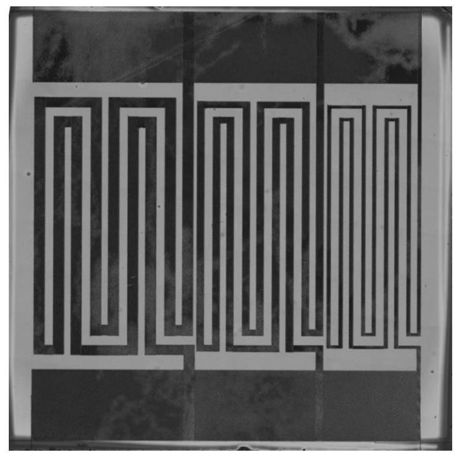
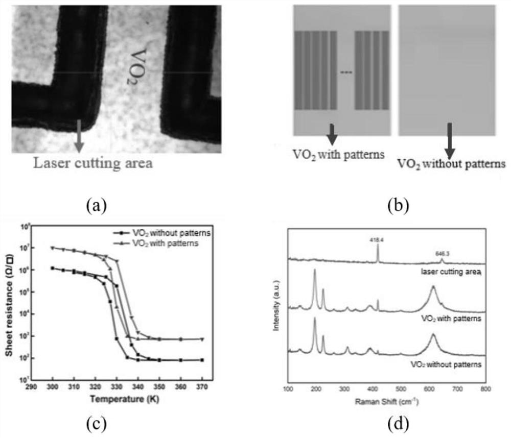
[0035] Step 4. adopting laser cutting to prepare the required graphics on the surface of the film sample obtained in step 3;
[0036] Step 5. Place the patterned sample in step 4 in a tube furnace and heat-treat it under a nitrogen-hydrogen mixed atmosphere. The specific process is: raise the temperature from room temperature to 440-460°C and keep it for 110-130min. Polymer pyrolysis to remove excess carbon in the film...
Embodiment 1
[0038] A method for preparing a patterned vanadium dioxide film, specifically comprising the following steps:
[0039] Step 1: Use the PAD method to prepare the vanadium ion precursor solution, wherein, take 0.0008 mol of polyethyleneimine (PEI), a water-soluble polymer raw material, and dissolve it uniformly in 50 mL of water, and then add 0.0008 mol of ethylenediaminetetraacetic acid to the solution (ethylene diamine tetraacetic acid, EDTA) and mix well, then add 0.0008 ammonium metavanadate (NH 4 VO 3 ) to stir evenly to obtain a polymer solution containing vanadium ions; pour the solution into an ultrafiltration cup, select an ultrafiltration membrane with a molecular weight of 10,000, add water to filter twice, and use a pinhole filter with a diameter of 13 mm and an aperture of 0.45 μm Obtain the precursor solution after filtering through the filter;
[0040]Step 2: Clean the silicon substrate, ultrasonically clean the substrate with acetone, absolute ethanol and deion...
PUM
| Property | Measurement | Unit |
|---|---|---|
| diameter | aaaaa | aaaaa |
| pore size | aaaaa | aaaaa |
| phase transition temperature | aaaaa | aaaaa |
Abstract
Description
Claims
Application Information
 - R&D
- Intellectual Property
- Life Sciences
- Materials
- Tech Scout
- Unparalleled Data Quality
- Higher Quality Content
- 60% Fewer Hallucinations
Browse by: Latest US Patents, China's latest patents, Technical Efficacy Thesaurus, Application Domain, Technology Topic, Popular Technical Reports.
© 2025 PatSnap. All rights reserved.Legal|Privacy policy|Modern Slavery Act Transparency Statement|Sitemap|About US| Contact US: help@patsnap.com


