Method for regulating and controlling thickness of two-dimensional Bi2O2Se thin film
A thin film thickness and thin film technology, applied in the field of Bi2O2Se thin film thickness regulation, can solve the problems of low gate control capability, small size, high dark current, etc., and achieve the effect of good repeatability and simple operation
- Summary
- Abstract
- Description
- Claims
- Application Information
AI Technical Summary
Problems solved by technology
Method used
Image
Examples
Embodiment 1
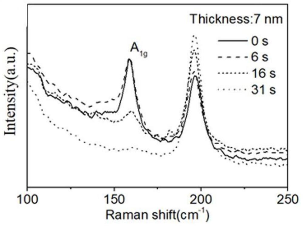
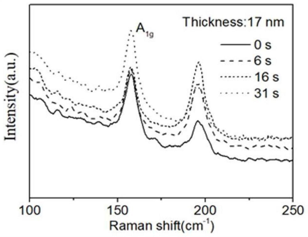
[0045] will be synthesized with Bi 2 o 2 The mica sheet of the Se film was placed in a reactive ion etching device. The rotational speed of the sample stage is 10 rpm, the rotation angle is -30°, the ion beam current is 80 mA, the ion beam voltage is 200 V, and the accelerating voltage is 200 V. The radio frequency power is 120W, the current of the neutralizer is 500mA, the incoming Ar flow rate is 10sccm, O 2 The flow rate was 6 sccm and the neutralizer gas (Ar) flow rate was 10 sccm. Vacuum up to 6.4×10 -4 Pa. A single etching time is 10s, etching is performed twice, and a total of 20s is etched. Such as figure 1 As shown, the atomic force microscope test shows that the sample is gradually thinned, and every etching 10s, the thinning is about 2nm, that is, 3 layers. The first etching can etch away thin irregular samples around and on the surface of the sample. Bi 2 o 2 The Se surface is flat and the RMS roughness changes little (0.33nm, 0.14nm, 0.26nm), which prove...
Embodiment 2
[0048] By HF wet transfer method, the two-dimensional Bi obtained on the mica substrate 2 o 2 Se film transferred to SiO 2 / Si substrate. Under the condition that other parameters remain unchanged, choose beam current 80mA, voltage 200V, etch twice, etching time is 15s, 12s, used to slowly thin the sample within 10nm, then choose beam current 100mA, voltage 280V, Etching 2 times, the etching time is 10s, 18s, used to thin the sample within 20nm. Such as Figure 4 As shown, the optical microscope observation shows that the etching effect is obvious. Figure 5 for Figure 4 Corresponding to the atomic force microscope test, 8nm is thinned to 3nm until it is completely etched; 14nm is thinned to 6nm.
Embodiment 3
[0050] By HF wet transfer method, the two-dimensional Bi obtained on the mica substrate 2 o 2 Se films were transferred onto Au / Si substrates. Under the parameter conditions in Example 1, etching was performed three times, and the etching time was 10s, 15s, and 19s, and a total of 44s was etched. Figure 6 Bi on Au / Si substrate 2 o 2 OM and corresponding AFM map of Se. Such as Figure 7 As shown, the Raman spectroscopy test results are consistent with figure 2 Similarly, it proves that the etching thinning rate of the sample after HF wet transfer is similar to that of the sample grown directly on mica, and the etching process does not significantly damage the sample.
PUM
 Abstract
Description
Claims
Application Information
 - R&D
- Intellectual Property
- Life Sciences
- Materials
- Tech Scout
- Unparalleled Data Quality
- Higher Quality Content
- 60% Fewer Hallucinations
Browse by: Latest US Patents, China's latest patents, Technical Efficacy Thesaurus, Application Domain, Technology Topic, Popular Technical Reports.
© 2025 PatSnap. All rights reserved.Legal|Privacy policy|Modern Slavery Act Transparency Statement|Sitemap|About US| Contact US: help@patsnap.com


