Pain receptor constructed based on indium sulfide film and application of pain receptor
A technology of susceptor and indium sulfide, applied in electrical components, physical realization, biological neural network models, etc., can solve problems such as Moore's Law is difficult to continue, transistor miniaturization, etc., and achieve the effect of good photoelectric characteristics
- Summary
- Abstract
- Description
- Claims
- Application Information
AI Technical Summary
Problems solved by technology
Method used
Image
Examples
Embodiment 1
[0050] 1. Using physical vapor deposition method, in a horizontal tube furnace with a single constant temperature zone to prepare large-area two-dimensional In 2 S 3 Continuous film (with an area range of 1cm×1cm);
[0051] 2. Weigh 20mg of In 2 S 3 Powder (99.99%, Aladdin), placed in the quartz boat, and the quartz boat is placed in the central constant temperature zone of the horizontal tube furnace (the temperature range is 950 ~ 1000 ℃);
[0052] 3. Use scotch tape to peel off the fluorphlogopite mica sheet with a size of 1cm×2cm: First, stick one side of the fluorphlogopite mica sheet on the scotch tape, and then use a clean blade to cut a small opening on the side of the fluorphlogopite mica sheet substrate, Due to the good dissociation properties of the fluorophlogopite, the fluorophlogopite can be easily peeled off into two clean and clean mica pieces. Use the side that has just been dissociated as the front side of the fluorophlogopite, and the fluorophlogopite is ...
Embodiment 2
[0056] The large-area two-dimensional In obtained in Example 1 2 S 3 Continuous thin film transfer to Si / SiO 2 on the substrate, with In 2 S 3 The thin film is the channel material, using photolithography and evaporation process, in In 2 S 3 Au metal with a thickness of 50nm is vapor-deposited on the film as the device electrode, and the length of the channel is 0.1-50 μm (preferably 10 μm), which is made into In 2 S 3 Membrane pain receptors.
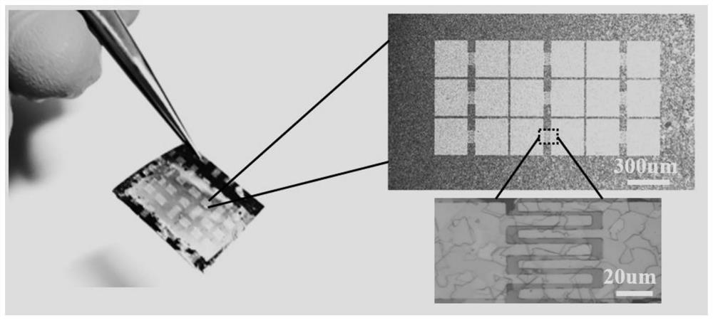
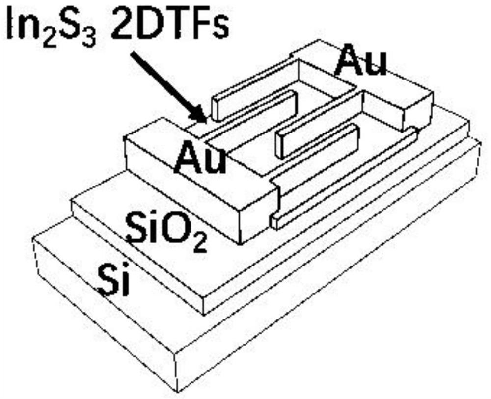
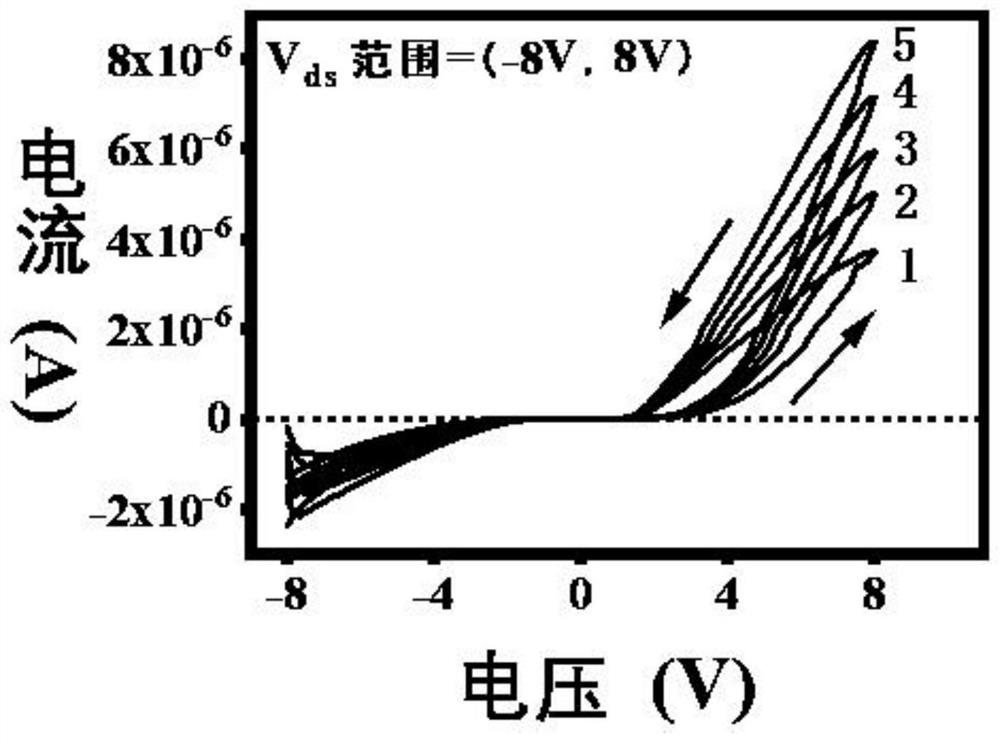
[0057] figure 1 For the In prepared in Example 2 2 S 3 The physical picture (left) of a thin film nociceptor and its local optical microscope magnification (right). Among them, the magnified image of the optical microscope (upper right) is In 2 S 3 Nine device assemblies on the film, the size of a single nociceptor is 500 μm × 300 μm; the magnified image of a local optical microscope (bottom right) is a channel map of a single nociceptor. The channel has a length of 50 μm and a width of 5 μm. figure 2 For the In prepared...
Embodiment 3
[0059] When the voltage pulse acts as an external stimulus signal, the In 2 S 3 Thin-film nociceptors mimic specific functions of artificial nociception. in 2 S 3The two ends of the electrodes of the thin film pain receptors input voltage pulse stimulation, and at the same time output the response current of the device; in particular, when the pulse voltage is gradually increased from 0V to 0.75V, the pain receptors will change from a non-responsive state to a stable response state. The voltage at this time is the "threshold" of the device; when the pain receptor is stimulated by a long-term (1200s) 1V voltage pulse, the response current will gradually increase from the stage (300-900s) to the saturation stage (900-1200s). Corresponding to the "inadaptive behavior" of pain receptors; the control voltage pulse of 8V is turned on for a period of time (45s) and then suddenly turned off, the response current will not disappear immediately, but the process of gradual relaxation ...
PUM
| Property | Measurement | Unit |
|---|---|---|
| thickness | aaaaa | aaaaa |
| length | aaaaa | aaaaa |
| wavelength | aaaaa | aaaaa |
Abstract
Description
Claims
Application Information
 - R&D Engineer
- R&D Manager
- IP Professional
- Industry Leading Data Capabilities
- Powerful AI technology
- Patent DNA Extraction
Browse by: Latest US Patents, China's latest patents, Technical Efficacy Thesaurus, Application Domain, Technology Topic, Popular Technical Reports.
© 2024 PatSnap. All rights reserved.Legal|Privacy policy|Modern Slavery Act Transparency Statement|Sitemap|About US| Contact US: help@patsnap.com


