


Quick Research
Generate reliable direction feasibility study reports for your R&D in just a few steps.

Technical Q&A
Discover and master advanced knowledge NOW. Basics, ideas, possibilities, all at once.

Find Solutions
As an expert in R&D theories, this can generate solutions to your technical problems instantly.

Evaluate Feasibility
Analyze your overall solution with one click, know your potential R&D risks in advance.

Monitor Landscape
Get weekly tech updates, stay abreast of the latest tech innovations and key insights.
SiC MOSFET device integrating groove and body plane gate
A planar gate and trench technology, applied in semiconductor devices, electrical components, circuits, etc., can solve problems such as device reliability degradation, achieve the effects of improving robustness, improving device switching performance, and reducing device gate charge
- Summary
- Abstract
- Description
- Claims
- Application Information
AI Technical Summary
Problems solved by technology
Method used
Image

Examples
Embodiment 1
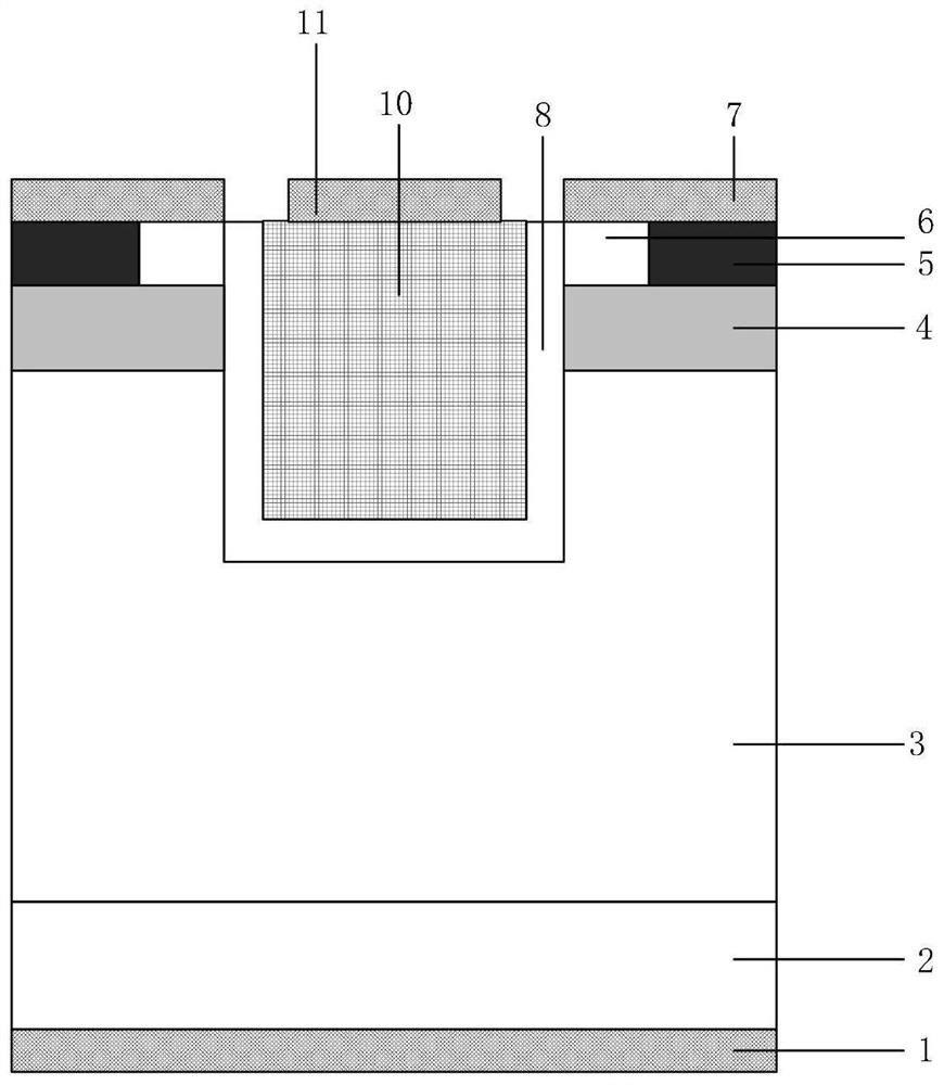
[0049] Such as figure 1 and figure 2 As shown, the structure of the present invention compared with the traditional trench gate MOSFET is as follows, including drain metal contact region 1, N+ substrate 2, N-drift region 3, P-body region 4, P+ source region 5, N+ source region 6, source Metal 7, insulating dielectric layer 8, P+ polysilicon 10, gate metal contact region 11.
[0050] The drain metal contact region 1 is located on the lower surface of the N+ substrate layer 2 .
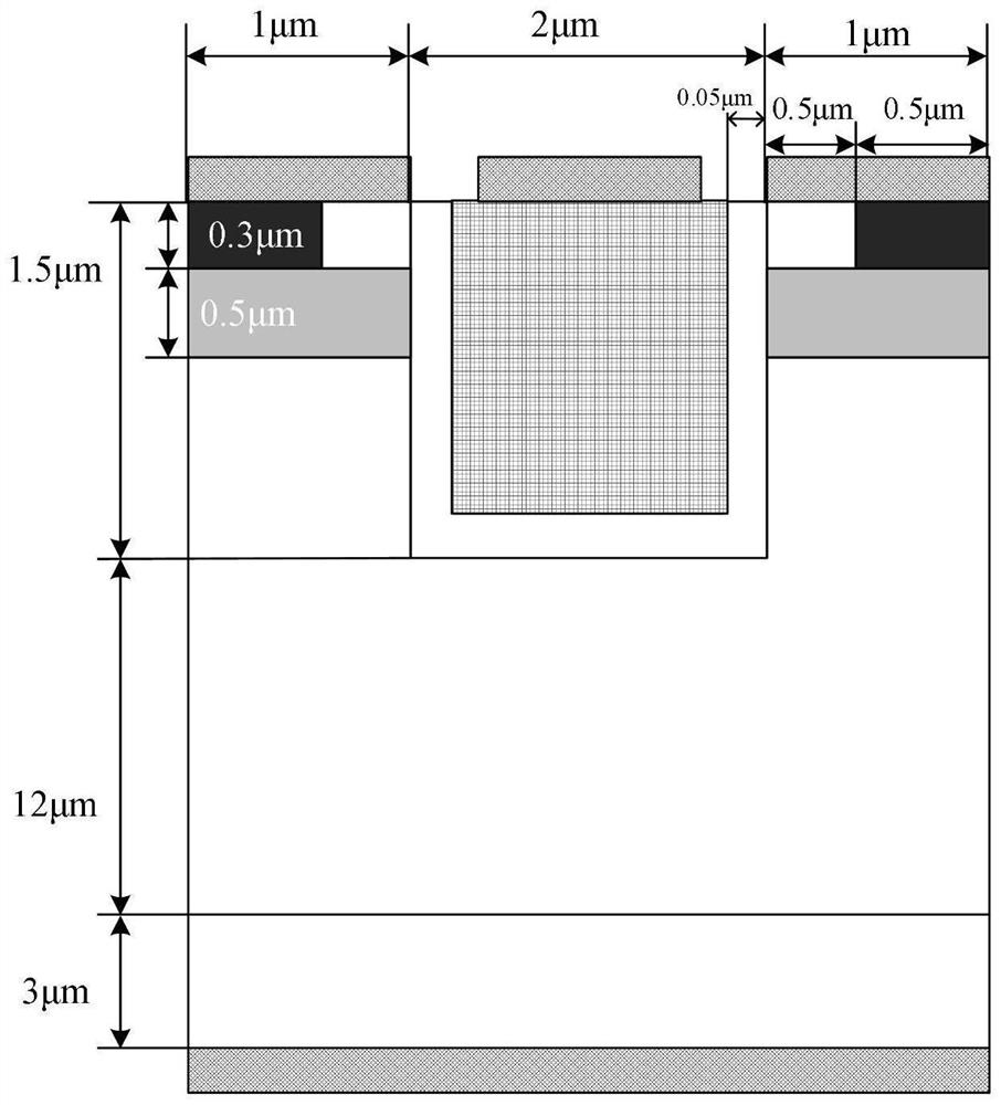
[0051] The N+ substrate layer 2 is located on the lower surface of the N-drift region 3 and the upper surface of the drain metal contact region 1; the length in the horizontal direction is 4 μm, and the length in the vertical direction is 3 μm; the doped N-type impurity concentration is 2×10 19 cm -3 .
[0052] The N-drift region 3 is located on the lower surface of the P-body region 4, the lower surface and the outer lower surface of the insulating dielectric layer 8, and is also located on the up...
Embodiment 2
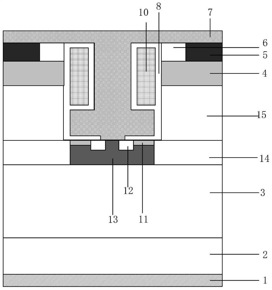
[0061] Such as image 3 and Figure 4 As shown, the present invention relates to a SiC MOSFET device structure of an improved SiC MOSFET device integrating a trench gate and a body planar gate. The device includes a drain metal contact region 1, an N+ substrate 2, an N-drift region 3, a P- Body region 4, P+ source region 5, N+ source region 6, source metal 7, insulating dielectric layer 8, P+ polysilicon 10, gate metal contact region 10, gate bottom channel region 11, gate bottom N+ source region 12, gate bottom P electric field shielding region 13 , current spreading region 14 , and second drift region 15 .
[0062] The drain metal contact region 1 is located on the lower surface of the N+ substrate 2 .
[0063] The N+ substrate layer 2 is respectively located on the lower surface of the N- drift region 3 and the upper surface of the cathode metal contact region 1; the length in the horizontal direction is 4 μm, and the length in the vertical direction is 3 μm; the doped N-...
PUM
| Property | Measurement | Unit |
|---|---|---|
| Side wall thickness | aaaaa | aaaaa |
| Thickness | aaaaa | aaaaa |
Abstract
Description
Claims
Application Information
 - R&D Engineer
- R&D Manager
- IP Professional
- Industry Leading Data Capabilities
- Powerful AI technology
- Patent DNA Extraction
Browse by: Latest US Patents, China's latest patents, Technical Efficacy Thesaurus, Application Domain, Technology Topic, Popular Technical Reports.
© 2024 PatSnap. All rights reserved.Legal|Privacy policy|Modern Slavery Act Transparency Statement|Sitemap|About US| Contact US: help@patsnap.com