Metal interconnection structure and bonding method thereof

A metal interconnection and bonding technology, applied in electrical components, electrical solid devices, circuits, etc., can solve the problems of low specific heat capacity, unfavorable chip operation with large workload, and nitrogen-doped silicon carbide material heating, etc., to prevent harmful diffusion, The effect of meeting the requirements of bonding strength and reducing the interface temperature

Pending Publication Date: 2021-11-02
ICLEAGUE TECH CO LTD
View PDF0 Cites 0 Cited by
  • Summary
  • Abstract
  • Description
  • Claims
  • Application Information

AI Technical Summary

Problems solved by technology

However, in the prior art, nitrogen-doped silicon carbide material is often used as the bonding interface. Although it can provide better bonding strength and can block the diffusion of metal copper, nitrogen-doped silicon carbide material as a dielectric layer has better properties than silicon dioxide. Low specific heat capacity, when a three-dimensional stacked chip is working, the heat generated by a certain current passing through the copper pillar will make the nitrogen-doped silicon carbide material heat up higher, which is not conducive to the long-term and heavy-duty operation of the chip

Method used


Image

  • Metal interconnection structure and bonding method thereof
  • Metal interconnection structure and bonding method thereof
  • Metal interconnection structure and bonding method thereof

Examples


Embodiment Construction

[0011] The specific embodiments of the metal interconnection structure and the bonding method of the metal interconnection structure provided by the present invention will be described in detail below with reference to the accompanying drawings.

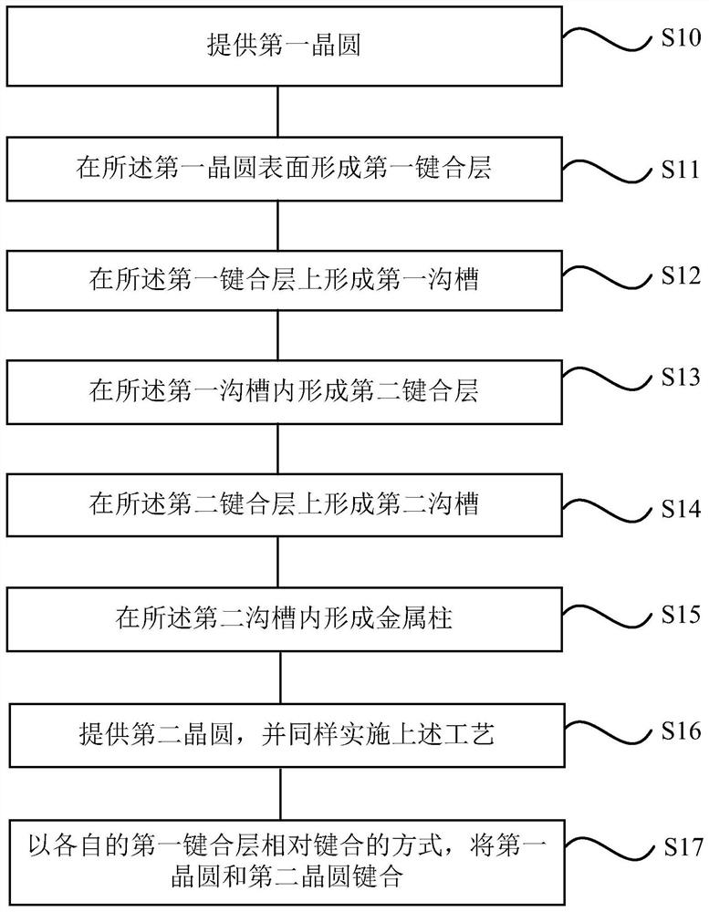
[0012] attached figure 1 Shown is a schematic diagram of a specific embodiment of the present invention. The bonding method of the metal interconnect structure includes: step S10, providing a first wafer; step S11, forming a first bonding layer on the surface of the first wafer ; Step S12, forming a first trench on the first bonding layer; Step S13, forming a second bonding layer in the first trench; Step S14, forming on the second bonding layer second trenches; step S15, forming metal pillars in the second trenches; step S16, providing a second wafer, and performing the same process; step S17, relatively bonding the first bonding layers manner, the first wafer and the second wafer are bonded.

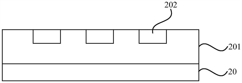
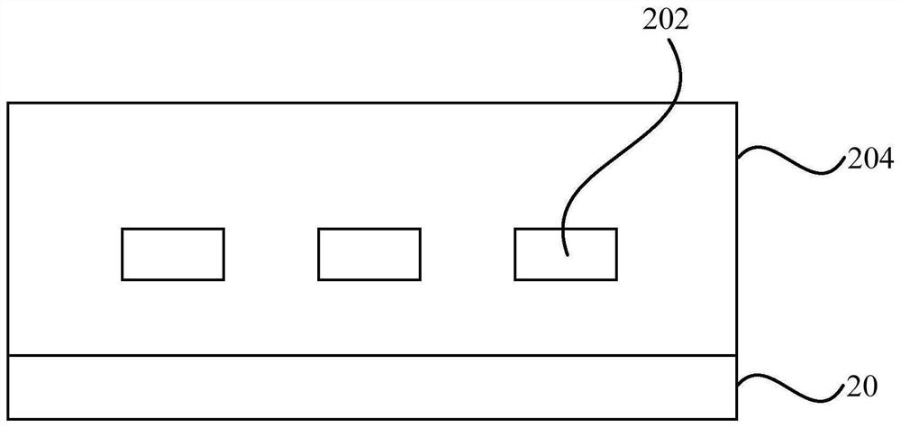
[0013] attached Figure 2A , referr...


PUM


Abstract

The invention provides a metal interconnection structure and a bonding method thereof. The structure comprises: a metal column which comprises a bonding interface; a first bonding layer which wraps the metal column, and is made of a silicon dioxide material; and a second bonding layer which is arranged around the bonding interface of the metal column to form an isolated annular structure, and is made of a nitrogen-doped silicon carbide material. According to the metal interconnection structure and the bonding method thereof, the nitrogen-doped silicon carbide material and the silicon dioxide are adopted as the bonding layers at the same time, and when two wafers or multiple wafers are stacked in three-dimensional stacking, under the condition that the chip function can be met, the bonding strength requirement can be met, harmful diffusion of connecting line copper can be prevented, and the interface temperature of the three-dimensional stacked chip during working can be reduced at the same time.

Description

technical field [0001] The present invention relates to the field of semiconductors, and in particular, to a metal interconnection structure and a bonding method of the metal interconnection structure. Background technique [0002] In the prior art, a three-dimensional stacking process is often used in the preparation process of chips, and two wafers of different functional devices are bonded together by generating covalent chemical bonds, so as to achieve the purpose of interconnection of different functional devices. Among them, the hybrid bonding process has a wide range of applications. However, in the prior art, nitrogen-doped silicon carbide materials are often used as the bonding interface. Although it can provide better bonding strength and can block the diffusion of metal copper, nitrogen-doped silicon carbide materials as a dielectric layer have more advantages than silicon dioxide. Low specific heat capacity, when the three-dimensional stacked chip is working, th...

Claims


Application Information

Patent Timeline
Patent Type & Authority Applications(China)
IPC IPC(8): H01L23/482H01L21/60
CPCH01L23/4824H01L23/4827H01L24/03H01L24/82H01L2224/03462H01L2224/0345H01L2224/03452
Inventor 邢程刘伟杰
Owner ICLEAGUE TECH CO LTD
Why Eureka
Try Eureka