Miniature snapshot spectrometer
A spectrometer and miniature technology, used in instruments, scientific instruments, spectrum surveys, etc., can solve the problems of limited spectral resolution, reduced temporal resolution, low resolution, etc., to reduce packaging time and cost, shock resistance and poor reliability, The effect of reducing the difficulty of mutual alignment
- Summary
- Abstract
- Description
- Claims
- Application Information
AI Technical Summary
Problems solved by technology
Method used
Image
Examples
Embodiment 1
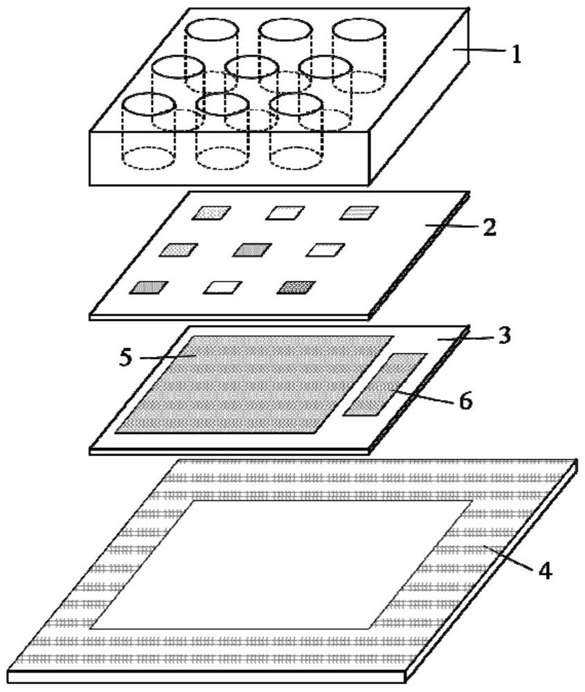
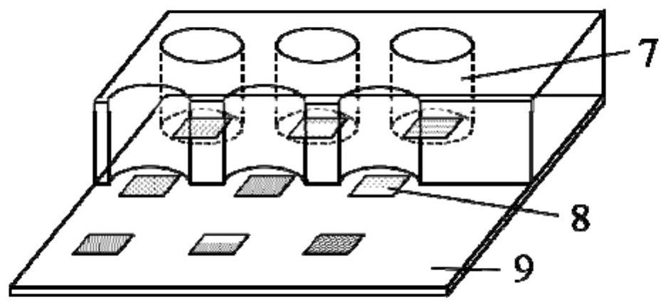
[0038] The substrate material of the angle filter 1 is a single crystal silicon circle with a thickness of about 1mm. A circular through-hole array is formed by deep silicon etching. The through-hole period is 20μm and the diameter is 16μm, which realizes the angle selection of the incident light within ~1°;
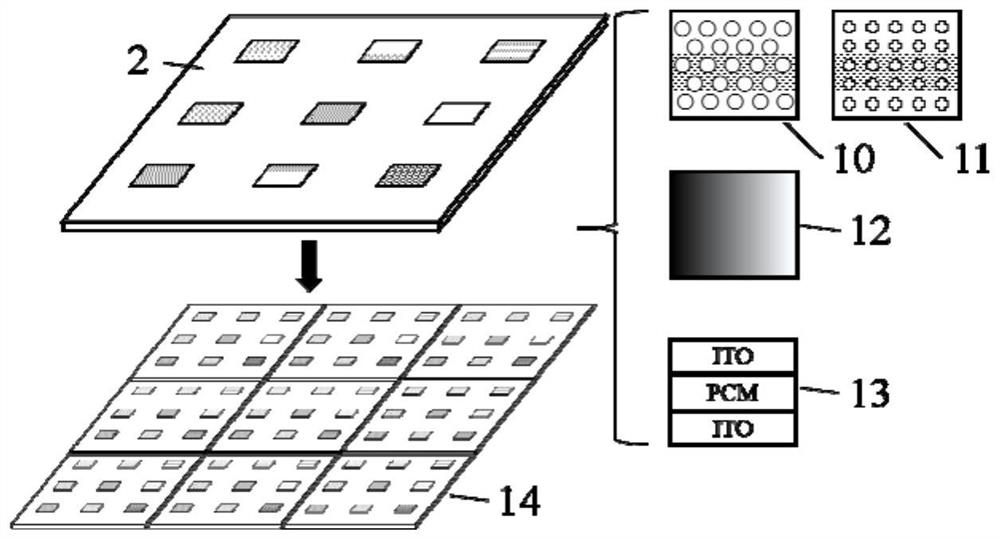
[0039] The band-selecting transparent medium substrate 9 of the spectrum-selective layer 2 is a 0.3 mm thick quartz wafer. Deposit a GSS film with a thickness of about 500nm on its back, use photolithography to generate 36 micro-nano structures 8 with different periods and transmission spectra, and photonic crystal arrays 10 on the photoresist, and use the dry etching process The structure is transferred to the GSS thin film layer to generate a nanoporous structure, and the target spectral response range is 450-750nm. The period of the photonic crystal nanohole is 300-600nm, the diameter is 100-300nm, the angle between the directions of the two periods is 30°-90°, and th...
Embodiment 2
[0046] The substrate material of the angle filter 1 is metal Al with a thickness of about 5 mm. A circular through-hole array is formed by wet etching. The through-hole period is 100 μm and the diameter is 80 μm, which realizes the angle selection of the incident light within ~1°;
[0047] The selective band transparent medium substrate 9 of the spectrum selective layer 2 is 0.5 mm thick CaF 2 substrate. A GSST film about 1 μm thick is deposited on its back, and 36 micro-nano structures 8 with different shapes and transmission spectra are formed on the photoresist by using ultraviolet lithography. The process transfers the structure to the GSST thin film layer to generate a metasurface structure, and the target spectral response range is 3.5-5 μm. The period of the metasurface structure is 2 μm, and the size of the structure is about 80 μm. Each group of different metasurfaces has a pitch of 100 um, which corresponds to the period of the through-hole structure of the upper a...
PUM
| Property | Measurement | Unit |
|---|---|---|
| Thickness | aaaaa | aaaaa |
| Thickness | aaaaa | aaaaa |
| Thickness | aaaaa | aaaaa |
Abstract
Description
Claims
Application Information
 - R&D
- Intellectual Property
- Life Sciences
- Materials
- Tech Scout
- Unparalleled Data Quality
- Higher Quality Content
- 60% Fewer Hallucinations
Browse by: Latest US Patents, China's latest patents, Technical Efficacy Thesaurus, Application Domain, Technology Topic, Popular Technical Reports.
© 2025 PatSnap. All rights reserved.Legal|Privacy policy|Modern Slavery Act Transparency Statement|Sitemap|About US| Contact US: help@patsnap.com


