
Semiconductor structure and forming method thereof

A semiconductor and isolation structure technology, applied in the field of semiconductor structure and its formation, can solve the problems of insufficient remaining thickness of the hard mask layer, narrowing of the sacrificial layer, uneven trench depth, etc., to reduce the impact of the etching process and avoid The effect of narrowing and consistent groove depth

Active Publication Date: 2021-10-22
SEMICON MFG INT (SHANGHAI) CORP +1
View PDF5 Cites 2 Cited by
  • Summary
  • Abstract
  • Description
  • Claims
  • Application Information

AI Technical Summary

Problems solved by technology

[0005] This application aims to solve the technical problems of narrowing of the sacrificial layer, non-uniform trench depth and / or insufficient remaining thickness of the hard mask layer during the fabrication of CFETs

Method used


Image

  • Semiconductor structure and forming method thereof
  • Semiconductor structure and forming method thereof
  • Semiconductor structure and forming method thereof

Examples


Embodiment Construction

[0040] As mentioned in the background, the prior art CFET formation method needs to be improved.

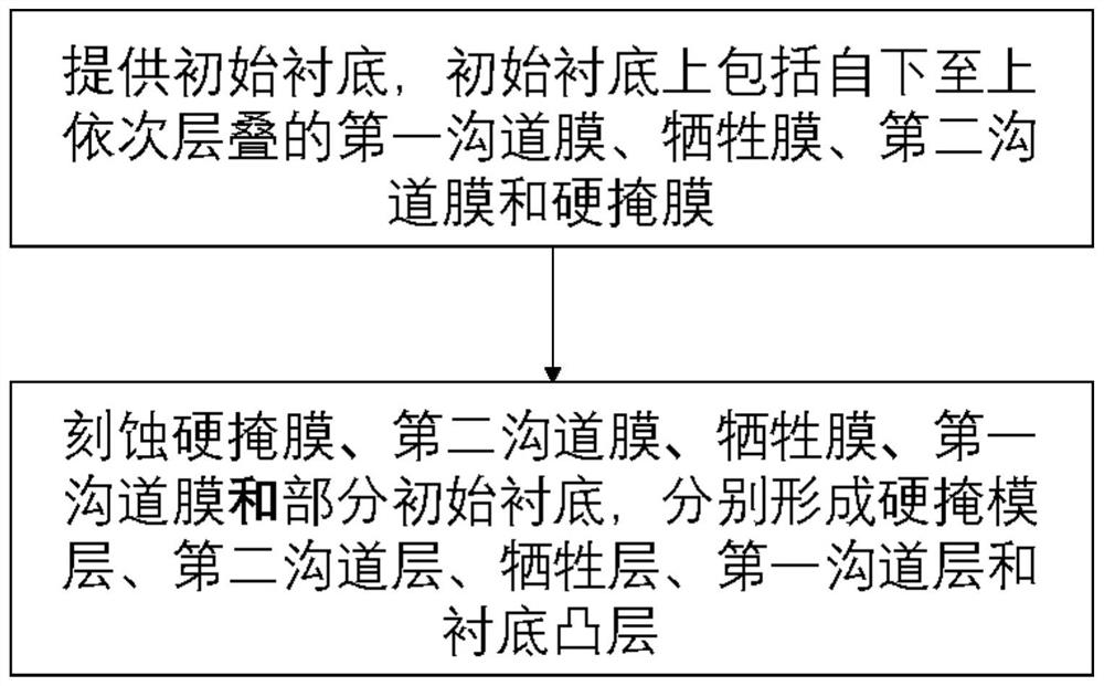
[0041] figure 1 A flowchart of a method for forming a semiconductor structure is shown, the method includes: providing an initial substrate, the initial substrate includes a first channel film, a sacrificial film, a second channel film and a first channel film stacked sequentially from bottom to top. Hard mask: etching the hard mask, the second channel film, the sacrificial film, the first channel film and part of the initial substrate to form a hard mask layer, a second channel channel layer, sacrificial layer, first channel layer and substrate convex layer.

[0042] Through the above method can be formed as figure 2 The semiconductor structure shown includes a substrate 1, a substrate convex layer 2 above the substrate 1, a first channel layer 4 above the substrate convex layer 2, and a channel layer above the first channel layer 4. The second channel layer 6 and the hard m...


PUM

PropertyMeasurementUnit
thicknessaaaaaaaaaa
thicknessaaaaaaaaaa
thicknessaaaaaaaaaa

Abstract

The invention discloses a semiconductor structure and a forming method thereof. The method comprises the steps that: an initial substrate is provided, wherein the initial substrate comprises a first sacrificial film, a first channel film, a second sacrificial film, a second channel film and a third sacrificial film which are sequentially stacked from bottom to top; the third sacrificial film and the second channel film are etched until the surface of the second sacrificial film is exposed to form a third sacrificial layer and a second channel layer; a first protection layer is formed on the side wall of the second channel layer; the second sacrificial film and the first channel film are etched until the surface of the first sacrificial film is exposed to form a second sacrificial layer and a first channel layer; a second protection layer is formed on the side wall of the second channel layer, the side wall of the second sacrificial layer and the side wall of the first channel layer; and the first sacrificial film and a part of the initial substrate are etched to enable the first sacrificial film to form a first sacrificial layer. According to the semiconductor structure and the forming method thereof disclosed by the invention, the CFET manufacturing process is improved, and the performance of the semiconductor structure is improved.

Description

technical field [0001] The present application relates to the field of semiconductor manufacturing, in particular to a semiconductor structure and a method for forming the same. Background technique [0002] The gate of a traditional FinFET (Fin Field Effect Transistor) only surrounds the channel region on three sides, and the bottom of the gate is connected to the semiconductor substrate, which may cause leakage current when the FinFET is turned off. For this reason, a kind of Complementary Field Effect Transistor (CFET, Complementary Field Effect Transistor) is proposed in the prior art, which adopts the gate surround technology, and the channels of the n-type field effect transistor and the p-type field effect transistor in the sheet form The regions are stacked one above the other and the gate completely surrounds the channel region, which not only effectively solves the problem of leakage current, but also reduces the size of the transistor by nearly one-third. [0003...

Claims


Application Information

Patent Timeline
Patent Type & Authority Applications(China)
IPC IPC(8): H01L21/336H01L29/423H01L29/78H01L21/8238H01L27/092
CPCH01L29/66545H01L29/42356H01L29/78H01L21/8238H01L21/823807H01L27/092
Inventor 张海洋纪世良苏博
Owner SEMICON MFG INT (SHANGHAI) CORP
Learn More