Embedded three-dimensional structure micro heating plate, preparation method and gas sensor
A three-dimensional structure, micro-heating technology, applied in the shape of heating elements, instruments, scientific instruments, etc., can solve the problem of uneven deposition of sensing materials, and achieve the effects of convenient drip positioning, constant and uniform heat radiation, and reduced power consumption.
- Summary
- Abstract
- Description
- Claims
- Application Information
AI Technical Summary
Problems solved by technology
Method used
Image
Examples
Embodiment 1
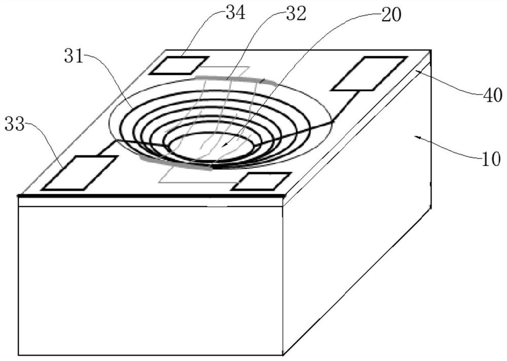
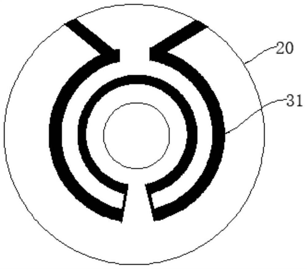
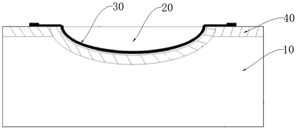
[0044] figure 1 It is a schematic structural view of the embedded three-dimensional structure micro-heating plate provided by Embodiment 1 of the present invention, figure 2 It is a top view of the concave cavity of the embedded three-dimensional structure micro-heating plate provided by Embodiment 1 of the present invention, image 3 It is a cross-sectional view of the embedded three-dimensional micro-heating plate provided by Embodiment 1 of the present invention. refer to Figure 1 to Figure 3 , a kind of built-in three-dimensional structure micro-heating board that the present embodiment provides, comprises silicon-based substrate 10 and electrode layer 30, and the surface layer of described silicon-based substrate 10 is provided with concave cavity 20, and the depth of described concave cavity 20 is 20-100μm. The electrode layer 30 includes a heating electrode 31 and a measuring electrode 32 , and the heating electrode 31 and the measuring electrode 32 are embedded in...
Embodiment 2
[0047] Figure 4 and Figure 5 It is a top view of the concave cavity of the embedded three-dimensional structure micro-heating plate provided by the second embodiment of the present invention, Figure 6 It is a cross-sectional view of the embedded three-dimensional structure micro-heating plate provided by the second embodiment of the present invention. refer to Figure 4 to Figure 6 , the concave cavity 20 is arranged on the upper surface of the silicon-based substrate 10, and the heating electrode pad 33 is arranged on the surface of the silicon-based substrate 10 adjacent to the outer edge of the concave cavity 20, and the heating electrode 31 is drawn out to the heating electrode Pad 33. The concave cavity 20 is in the shape of a truncated cone, and the heating electrodes 31 are arranged in a regular shape along the side wall or the sunken bottom of the concave cavity 20 . Such as Figure 4 As shown, the heating electrodes 31 are arranged in an "S" shape along the si...
Embodiment 3
[0052] Figure 7 It is a flow chart of the preparation method of the embedded three-dimensional structure micro-heating plate provided by the third embodiment of the present invention. refer to Figure 7 A method for preparing a built-in three-dimensional structure micro-heating plate provided in this embodiment comprises the following steps:
[0053] S1) Provide a silicon-based substrate.
[0054] The silicon-based substrate is preferably a 4-inch n-type (100) silicon wafer with a thickness of 200-550 μm.
[0055] S2) Making a concave cavity on the surface layer of the silicon-based substrate.
[0056] A window pattern is formed on the surface of the silicon-based substrate by a photolithography process, and the concave cavity is etched in the window pattern area by an ion etching process under the protection of a photoresist. Specifically, chemical vapor deposition is used to form a silicon oxide film with a thickness of 500nm on the surface of the silicon wafer, and the...
PUM
| Property | Measurement | Unit |
|---|---|---|
| depth | aaaaa | aaaaa |
| thickness | aaaaa | aaaaa |
| thickness | aaaaa | aaaaa |
Abstract
Description
Claims
Application Information
 - R&D
- Intellectual Property
- Life Sciences
- Materials
- Tech Scout
- Unparalleled Data Quality
- Higher Quality Content
- 60% Fewer Hallucinations
Browse by: Latest US Patents, China's latest patents, Technical Efficacy Thesaurus, Application Domain, Technology Topic, Popular Technical Reports.
© 2025 PatSnap. All rights reserved.Legal|Privacy policy|Modern Slavery Act Transparency Statement|Sitemap|About US| Contact US: help@patsnap.com


