
A silicon-based detector with gradually changing width and its preparation method

A detector and silicon-based technology, applied in the field of optical interconnection, can solve the problems of difficult to meet the optical absorption length, large series resistance of devices, and low optical responsivity at the same time, achieve high bandwidth, high responsivity, and increase saturated optical power Effect

Active Publication Date: 2022-04-22
INST OF SEMICONDUCTORS - CHINESE ACAD OF SCI
View PDF0 Cites 0 Cited by
  • Summary
  • Abstract
  • Description
  • Claims
  • Application Information

AI Technical Summary

Problems solved by technology

The first method needs to use an on-chip waveguide optical splitter for light splitting. The processing accuracy of the on-chip waveguide optical splitter is relatively high, the overall size of the device is relatively large, and the optical splitter itself has a certain amount of optical loss, resulting in The responsivity is low (Optics Express, 23(2015) 22857 22866.); the main problem of the second method is that although the side waveguide can homogenize the light field intensity in the detector, it is difficult to meet the effective light absorption length at the same time , so the photoresponsivity is also relatively low
The lateral waveguide occupies the lower electrode area of ​​the detector, resulting in a large series resistance of the device and limited bandwidth (Optics Letter, 42(2017) 851854.)

Method used


Image

  • A silicon-based detector with gradually changing width and its preparation method
  • A silicon-based detector with gradually changing width and its preparation method
  • A silicon-based detector with gradually changing width and its preparation method

Examples


Embodiment Construction

[0027] In order to make the object, technical solution and advantages of the present invention clearer, the present invention will be further described in detail below in conjunction with specific embodiments and with reference to the accompanying drawings.

[0028] The saturation characteristics of photodetectors are affected by thermal effects, space charge effects, and voltage division by series resistors. The thermal effect is determined by the structure of the device and the heat dissipation characteristics of the material, while the space charge effect and the series resistance voltage division can change the saturation characteristics of the device by changing the electric field strength of the depletion layer of the photodetector. The series resistance is determined by the device material and fabrication process. The space charge effect mainly depends on the structure of the photodetector. On the one hand, it is necessary to optimize the device structure to increase t...


PUM

PropertyMeasurementUnit
lengthaaaaaaaaaa
electrical resistivityaaaaaaaaaa

Abstract

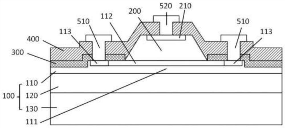
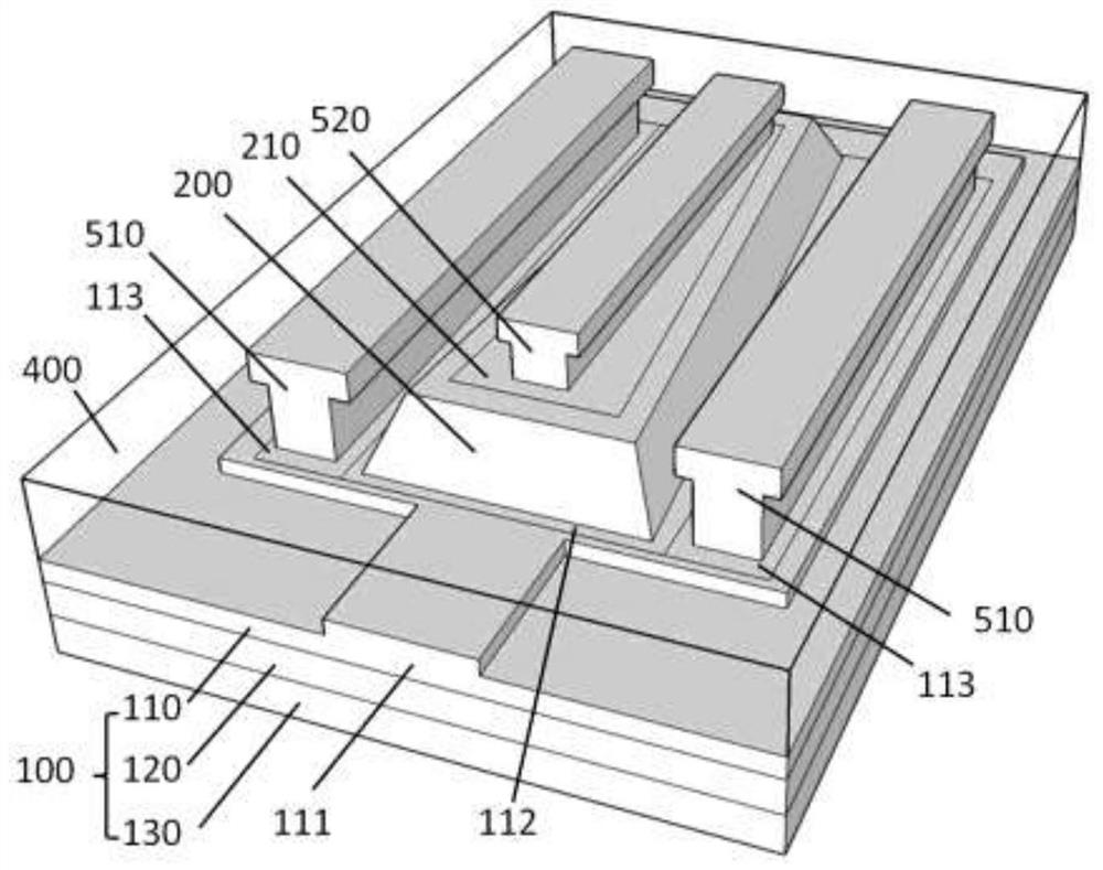
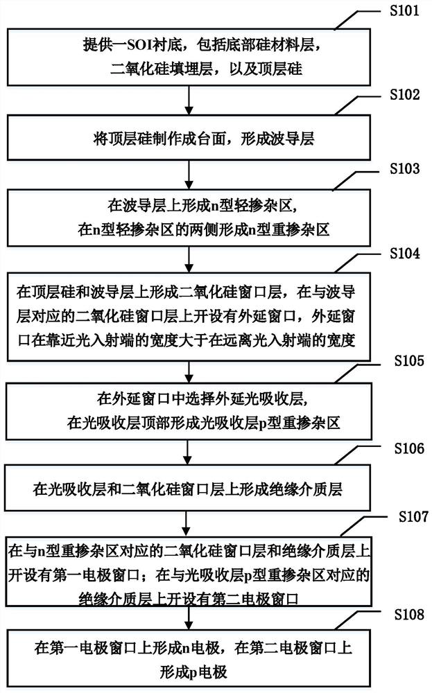
The invention discloses a silicon-based detector with gradually changing width, comprising: SOI substrate, including: a bottom silicon material layer, a silicon dioxide buried layer, a top layer of silicon, and a waveguide layer is formed on the top layer of silicon; an n-type lightly doped region , formed on the waveguide layer; the n-type heavily doped region, formed on both sides of the n-type lightly doped region; the light absorbing layer, formed on the n-type lightly doped region, part of the upper surface of the light absorbing layer is formed with light The p-type heavily doped region of the absorbing layer; the silicon dioxide window layer is formed on the top layer of silicon and the waveguide layer, and an epitaxial window is opened on the silicon dioxide window layer corresponding to the waveguide layer; the two corresponding to the n-type heavily doped region A first electrode window is opened on the silicon oxide window layer and the insulating medium layer; a second electrode window is opened on the insulating medium layer corresponding to the p-type heavily doped region of the light absorbing layer; an n electrode is formed on the first electrode window; The p-electrode is formed on the second electrode window; the width of the light absorbing layer near the light-incident end is greater than the width away from the light-incident end.

Description

technical field [0001] The invention relates to the field of optical interconnection, in particular to a silicon-based detector with gradually changing width and a preparation method thereof. Background technique [0002] High-frequency photonic links have the advantages of wide bandwidth, low transmission loss, small size, low weight, and strong anti-electromagnetic interference capabilities, which can effectively improve the transmission capacity and transmission rate of communication systems, and are widely favored in many microwave and millimeter wave applications , such as microwave photon radar, phased array antenna and ROF (radio-on-optical communication), etc. Low dark current, high speed, high responsivity and high saturation power photodetectors are crucial in RF (radio frequency) photonic links. Due to the limitation of the bandgap width of the silicon material, the working wavelength of the silicon detector is below 1100nm, which is not suitable for light detect...

Claims


Application Information

Patent Timeline
Patent Type & Authority Patents(China)
IPC IPC(8): H01L31/075H01L31/0352H01L31/18
CPCH01L31/035281H01L31/1844H01L31/1808H01L31/1812H01L31/075Y02E10/548Y02P70/50
Inventor 刘智成步文郑军薛春来
Owner INST OF SEMICONDUCTORS - CHINESE ACAD OF SCI
Learn More