


Quick Research
Generate reliable direction feasibility study reports for your R&D in just a few steps.

Technical Q&A
Discover and master advanced knowledge NOW. Basics, ideas, possibilities, all at once.

Find Solutions
As an expert in R&D theories, this can generate solutions to your technical problems instantly.

Evaluate Feasibility
Analyze your overall solution with one click, know your potential R&D risks in advance.

Monitor Landscape
Get weekly tech updates, stay abreast of the latest tech innovations and key insights.
Interlayer dielectric cavity fault test structure and test method based on switched capacitor
A technology for interlayer dielectric and fault testing, applied in electronic circuit testing, measuring electricity, measuring devices, etc., can solve the problems of detection accuracy restriction and inapplicability, and achieve the effect of improving process and high testing accuracy.
- Summary
- Abstract
- Description
- Claims
- Application Information
AI Technical Summary
Problems solved by technology
Method used
Image

Examples
specific Embodiment approach 1
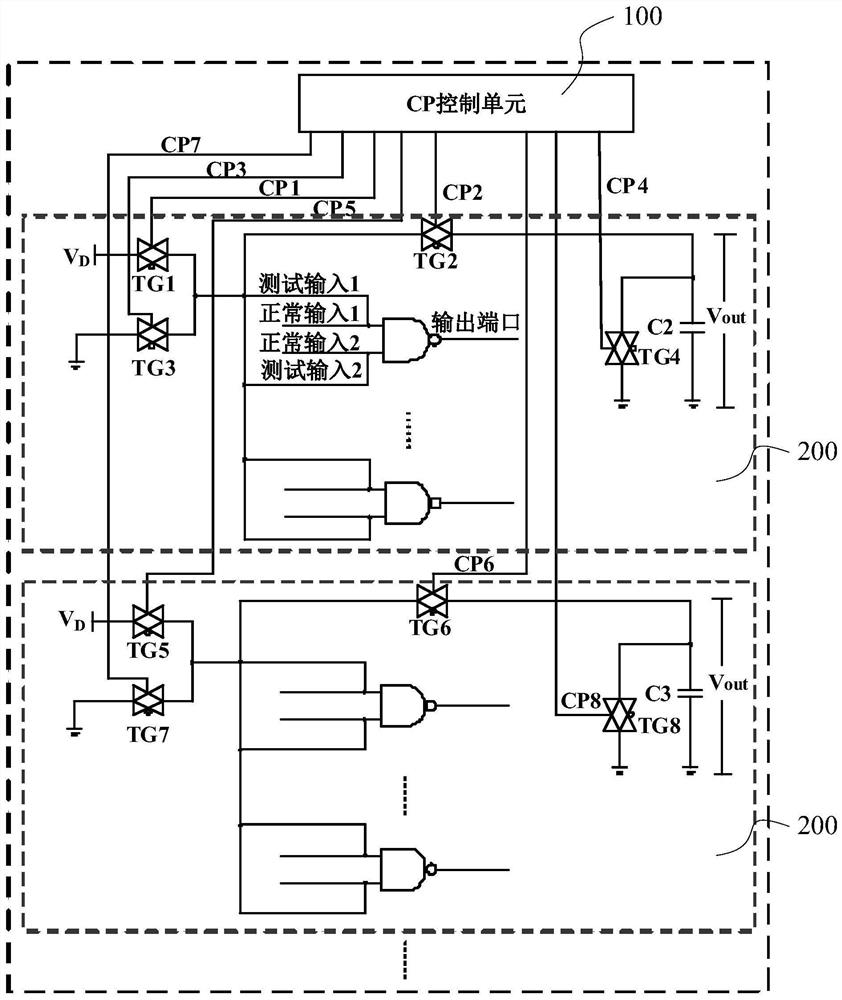
[0051] Specific implementation mode 1. Combination figure 1 As shown, the first aspect of the present invention provides a kind of interlayer dielectric void failure test structure based on switched capacitance, including CP control unit 100 and a plurality of test units 200;
[0052] Each test unit 200 includes a test capacitor and four transmission gate switches,
[0053] The CP control unit 100 is used to control the opening and closing of the four transmission gate switches in each test unit 200;
[0054] One end of the No. 1 transmission gate switch is connected to the power supply VD, and the other end is connected to the test input terminals of all the logic gates to be tested on the integrated circuit; one end of the No. 3 transmission gate switch is grounded, and the other end is connected to the test input terminals of all the logic gates to be tested; One end of the No. 4 transmission gate switch is connected to the test input terminals of all the logic gates to be...
specific Embodiment approach 2
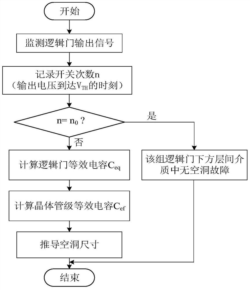
[0060] Specific embodiment two, combine Figure 1 to Figure 5 As shown, another aspect of the present invention also provides a method for testing interlayer dielectric void failure based on switched capacitors, which is implemented based on the structure for testing interlayer dielectric void faults based on switched capacitors described in the first specific embodiment,
[0061] Each test unit 200 realizes the same method for void fault testing;
[0062] The interlayer dielectric test structure involved in the method of the present invention is as figure 1 shown. Each test unit is responsible for monitoring the N logic gates on the upper layer of the ILD. A test unit contains a voltage of V D The DC power supply (V D The value is determined by the power supply voltage of the MOS tube), four transmission gate switches TG and a test capacitor with known capacitance value (the capacitance value of the test capacitor is C eq0 1000 times). The on and off of each transmission...
specific Embodiment
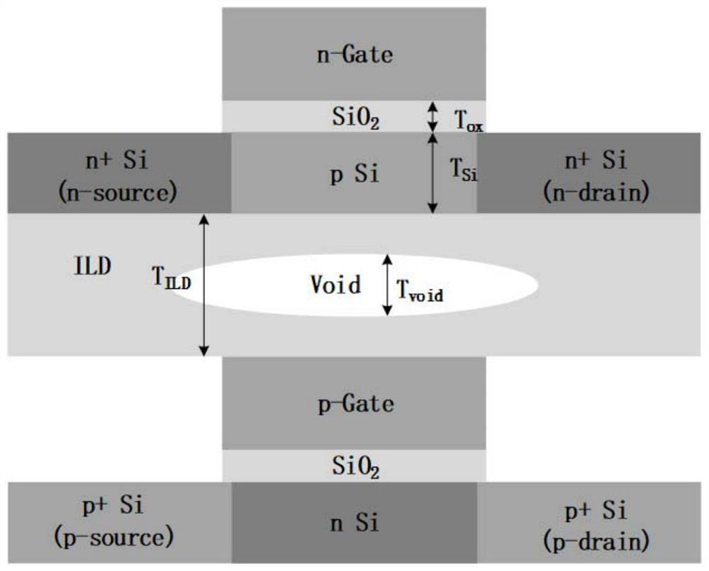
[0114] For the use of 22nm process, interlayer dielectric thickness T ILD For a 20nm M3D integrated circuit, the simulation process and derivation results of void fault detection are introduced in detail. The process parameters of the transistors inside the M3D integrated circuit are: T ox = 1 nm, T Si =6nm, W=300nm, L=22nm.
[0115] First, determine the quantity N=200 of a group of logic gates that can be monitored by a test unit 200, and calculate the equivalent capacitance value C of a group of logic gates on the ILD upper layer when there is no void fault eq0 . Taking the NAND gate as an example, the number of MOS transistors included in a logic gate is m=4. When there is no void fault inside the interlayer medium, according to C eq0 The solution formula can determine the equivalent capacitance C of the logic gate eq0 =7.935fF.
[0116] Second, determine the switch equivalent capacitance C S and the number of switching times n when there is no fault 0 . Build the...
PUM
 Abstract
Description
Claims
Application Information
 - R&D Engineer
- R&D Manager
- IP Professional
- Industry Leading Data Capabilities
- Powerful AI technology
- Patent DNA Extraction
Browse by: Latest US Patents, China's latest patents, Technical Efficacy Thesaurus, Application Domain, Technology Topic, Popular Technical Reports.
© 2024 PatSnap. All rights reserved.Legal|Privacy policy|Modern Slavery Act Transparency Statement|Sitemap|About US| Contact US: help@patsnap.com