Hybrid imaging detector chip based on semiconductor integrated circuit CMOS process

A technology of imaging detectors and integrated circuits, applied in the field of semiconductors

Active Publication Date: 2021-09-28
西安中科立德红外科技有限公司
View PDF6 Cites 4 Cited by
  • Summary
  • Abstract
  • Description
  • Claims
  • Application Information

AI Technical Summary

Problems solved by technology

[0003] With the development of industry and living standards, pure infrared imaging can no longer meet the demand, and imaging technology with wid...

Method used


Image

  • Hybrid imaging detector chip based on semiconductor integrated circuit CMOS process
  • Hybrid imaging detector chip based on semiconductor integrated circuit CMOS process
  • Hybrid imaging detector chip based on semiconductor integrated circuit CMOS process

Examples


Embodiment Construction

[0039] Reference will now be made in detail to the exemplary embodiments, examples of which are illustrated in the accompanying drawings. When the following description refers to the accompanying drawings, the same numerals in different drawings refer to the same or similar elements unless otherwise indicated. The implementations described in the following exemplary embodiments do not represent all implementations consistent with this application. Rather, they are merely examples of apparatuses and methods consistent with aspects of the present application as recited in the appended claims.

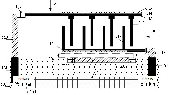
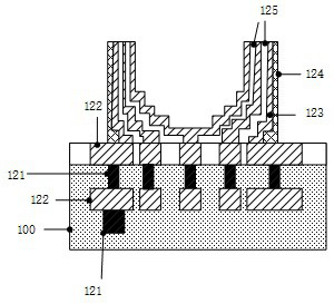
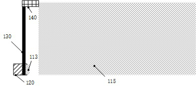
[0040] Such as Figure 1 to Figure 3 As shown, an embodiment of the present application provides a hybrid imaging detector chip based on a semiconductor integrated circuit CMOS process. The chip includes a substrate 100, an upper electrical connection support structure 120, an upper serpentine beam structure 130, a visible light sensing region 160, The CMOS reading circuit 150 on both s...


PUM


Abstract

The invention provides a hybrid imaging detector chip based on a semiconductor integrated circuit CMOS process. The chip comprises a substrate, a visible light sensing area located at the bottom of the substrate, CMOS reading circuits located on the two sides of the visible light sensing area, a suspended upper micro-bridge structure and a suspended lower micro-bridge structure which are both located at the top of the substrate, an air gap transistor formed between the lower micro-bridge structure and the substrate, an upper electric connection supporting structure, an upper snakelike beam structure, and a voltage variable resistor which is located at the contact position of the upper snakelike beam structure and the upper electric connection supporting structure. A diode is arranged in the visible light sensing area, and when the lower micro-bridge structure absorbs infrared light and shifts up and down to change the air gap height of the air gap transistor, the source-drain current of the air gap transistor is changed, so the induction of visible light and infrared light is realized.

Description

technical field [0001] The present application relates to the field of semiconductor technology, in particular to a hybrid imaging detector chip based on a semiconductor integrated circuit CMOS process. Background technique [0002] Infrared imaging sensor is a product widely used in the field of infrared detection technology. It generally adopts a microbridge structure integrated on a complementary metal oxide semiconductor (Complementary Metal Oxide Semiconductor, referred to as: CMOS) circuit, and uses a thermistor to absorb infrared rays. , and through the CMOS circuit, the changing signal is converted into an electrical signal to amplify and output, so as to realize the thermal imaging function. [0003] With the development of industry and living standards, pure infrared imaging can no longer meet the needs, and imaging technologies with wider bands have attracted more and more attention, especially imaging technologies that are sensitive to visible light and infrared ...

Claims


Application Information

Patent Timeline
IPC IPC(8): H01L27/146G01J1/46
CPCH01L27/14643H01L27/1465G01J1/46
Inventor 刘伟王鹏郭得福马仁旺段程鹏欧秦伟
Owner 西安中科立德红外科技有限公司
Why Eureka
Try Eureka