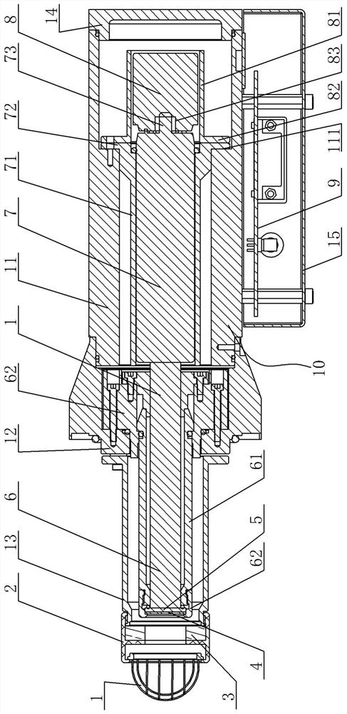
Scanning electron microscope electron detector with high collection efficiency
A collection efficiency, scanning electron microscope technology, applied in circuits, discharge tubes, electrical components, etc., can solve the problems of limited electronic signal receiving efficiency, poor signal-to-noise ratio, and signal escape.
- Summary
- Abstract
- Description
- Claims
- Application Information
AI Technical Summary
Problems solved by technology
Method used
Image

Examples
specific Embodiment
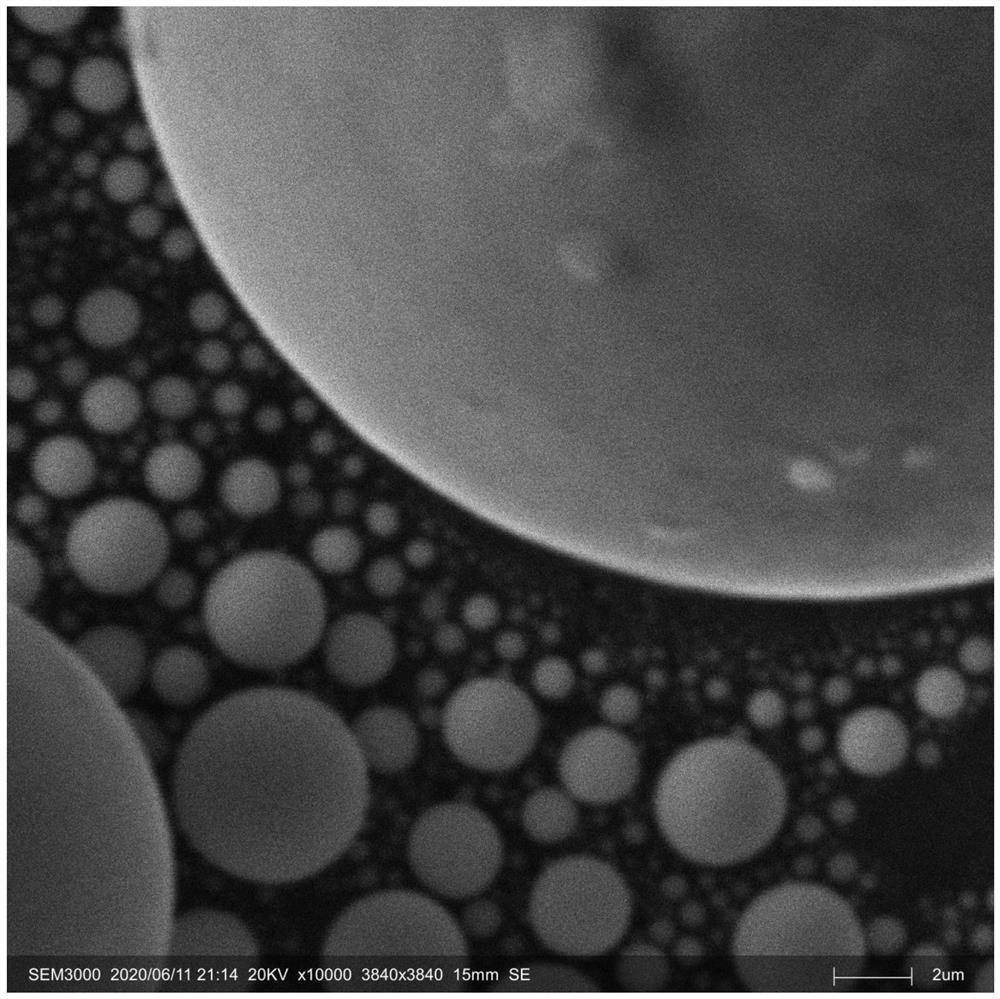
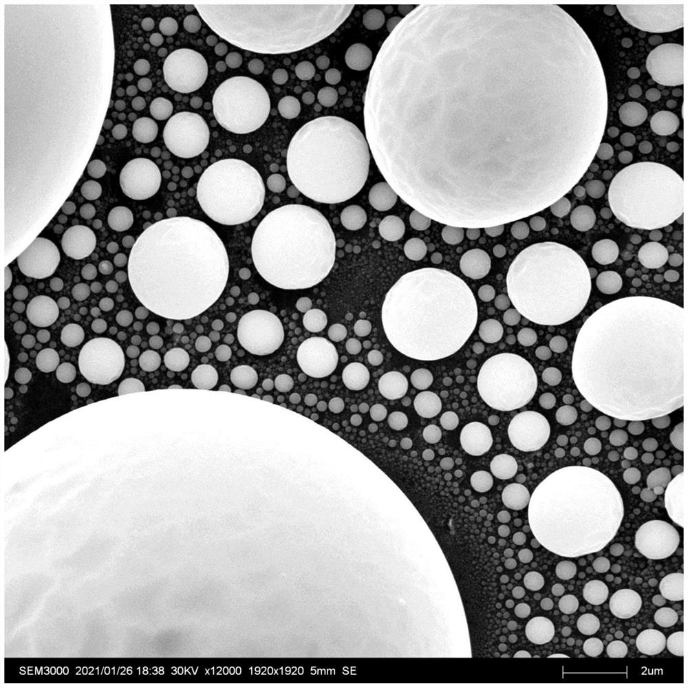
[0046] The specific embodiment detects: in the tungsten filament thermal emission scanning electron microscope, use the scanning electron microscope electronic detector of high collection efficiency, put the standard tin ball sample into the sample chamber, then vacuumize, after vacuum is finished, open the electron gun, will accelerate The voltage is set to 30kV, the working distance is 5mm, and the solder ball sample is observed under 12000x magnification after focusing and destigmatization. Acquire images (see image 3 ), it can be found that the image is clear, the edge is sharp, the contrast is obvious, and the imaging effect has been greatly improved. Therefore, in this case, the detection efficiency of the SEM electron detector is greatly improved.
PUM
 Abstract
Description
Claims
Application Information
 - R&D
- Intellectual Property
- Life Sciences
- Materials
- Tech Scout
- Unparalleled Data Quality
- Higher Quality Content
- 60% Fewer Hallucinations
Browse by: Latest US Patents, China's latest patents, Technical Efficacy Thesaurus, Application Domain, Technology Topic, Popular Technical Reports.
© 2025 PatSnap. All rights reserved.Legal|Privacy policy|Modern Slavery Act Transparency Statement|Sitemap|About US| Contact US: help@patsnap.com