
PCB pattern transfer alignment target method

A PCB board and graphics transfer technology, applied in the formation of electrical connections of printed components, electrical components, printed circuit manufacturing, etc., can solve the problems of reduced production efficiency, different diameters of alignment targets, etc., to improve alignment, The effect of improving production efficiency and improving uniformity

Pending Publication Date: 2021-09-17
GUANGZHOU MEADVILLE ELECTRONICS
View PDF9 Cites 0 Cited by
  • Summary
  • Abstract
  • Description
  • Claims
  • Application Information

AI Technical Summary

Problems solved by technology

[0005] In order to overcome the deficiencies of the prior art, one of the objectives of the present invention is to provide a PCB board pattern transfer alignment target method, which can solve the problems of different diameters of alignment targets and reduced production efficiency

Method used


Image

  • PCB pattern transfer alignment target method
  • PCB pattern transfer alignment target method
  • PCB pattern transfer alignment target method

Examples


Embodiment Construction

[0028] Below, the present invention will be further described in conjunction with the accompanying drawings and specific implementation methods. It should be noted that, under the premise of not conflicting, the various embodiments described below or the technical features can be combined arbitrarily to form new embodiments. .

[0029] It should be noted that when a component is said to be "fixed" to another component, it can be directly on the other component or there can also be an intervening component. When a component is said to be "connected" to another component, it may be directly connected to the other component or there may be intervening components at the same time. When a component is said to be "set on" another component, it may be set directly on the other component or there may be an intervening component at the same time. The terms "vertical," "horizontal," "left," "right," and similar expressions are used herein for purposes of illustration only.

[0030] Un...


PUM


Abstract

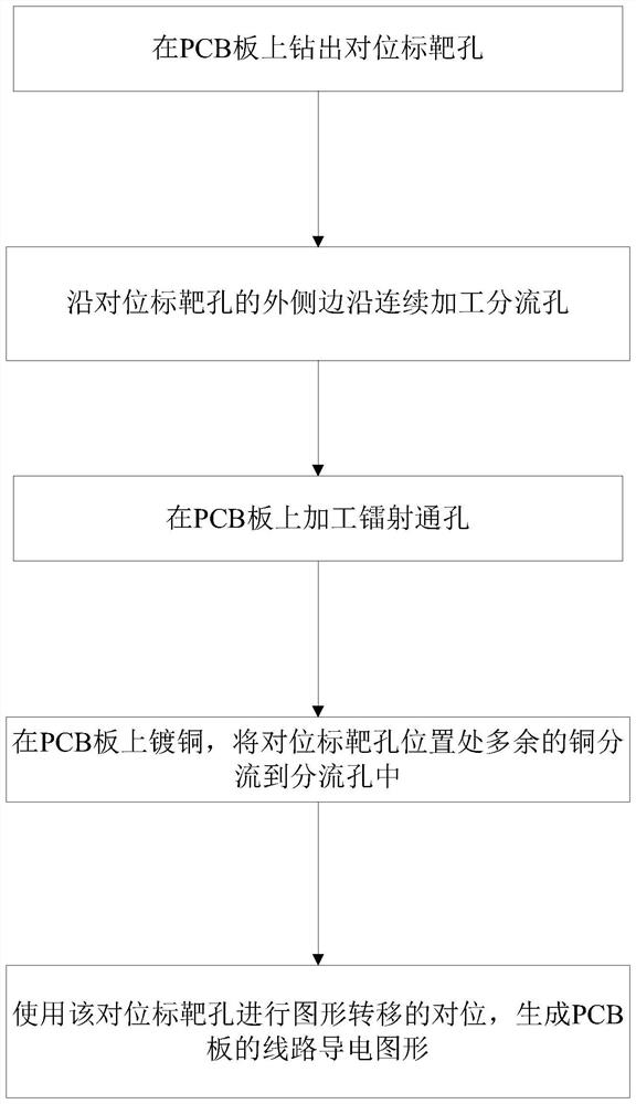
The invention discloses a PCB pattern transfer alignment target method. The method comprises the following steps: drilling alignment target holes in a PCB; continuously machining shunting holes along the edge of the outer side of the alignment target hole; processing a laser through hole in the PCB; carrying out copper plating on the PCB, and shunting redundant copper at the position of the alignment target hole into the shunting holes; and performing pattern transfer alignment by using the alignment target hole to generate a circuit conductive pattern of the PCB. In the copper plating process, the shunting holes are designed around the alignment target holes for protection, the effects of shunting the electroplating density and increasing the electroplating area are achieved in the complex waveform pulse electroplating process, the diameter consistency of the alignment target holes can be effectively protected, the stability is improved, and the influence of copper thickness protrusions is reduced; the uniformity of the copper thickness in the alignment target hole is improved, the product problems of exposure rejection, deviation of the pattern PAD and the laser hole and the like in the pattern transfer process are avoided, the production efficiency is improved, and the alignment degree of the pattern PAD and the laser hole is improved.

Description

technical field [0001] The invention relates to the field of circuit boards, in particular to a target method for transferring and aligning PCB graphics. Background technique [0002] At present, with the development of light, thin, short and small PCB boards, the design of laser holes is getting smaller and smaller, which is very easy to cause laser holes to collapse. Recently, the design of laser blind holes has developed to the level of laser drilled through hole design. (i.e. X-via). [0003] However, the existing pattern transfer alignment target method has the following defects: [0004] During the copper plating process for the alignment target hole, due to the uniform copper plating, copper thick bumps will be formed around the alignment target hole, which seriously affects the accuracy of the diameter of the alignment target hole, and alignment targets often appear. The problem of different diameters reduces the production efficiency and causes the bad defect of g...

Claims


Application Information

Patent Timeline
Patent Type & Authority Applications(China)
IPC IPC(8): H05K3/42
CPCH05K3/42H05K3/423
Inventor 张声芹姚晓建钮荣杰王宏业
Owner GUANGZHOU MEADVILLE ELECTRONICS
Learn More