Cutting steel wire surface treatment device for semiconductor wafer

A surface treatment device and technology for cutting steel wire, which is applied in the direction of thin material processing, grinding drive device, grinding/polishing safety device, etc., can solve the problems of heavy cutting steel wire, troublesome manual handling, poor processing effect, etc., and achieve convenient cleaning Cleans, prevents detachment, improves wiping effect

Inactive Publication Date: 2021-09-17
NANJING VOCATIONAL UNIV OF IND TECH
View PDF0 Cites 0 Cited by
  • Summary
  • Abstract
  • Description
  • Claims
  • Application Information

AI Technical Summary

Problems solved by technology

[0003] The purpose of the present invention is to provide a cutting wire surface treatment device for semiconductor wafers, to solve the problem that most of the cutting wire surface treatment devices proposed in the above-mentioned background technology have poor processing effects, and mechanically pre-process the steel wire surface before the steel wire surface treatment. Rust removal, and because the cut steel wire needs to be wound after surface treatment, it is convenient for subsequent wire drawing processing, but because the cut steel wire after winding is heavy, manual handling is more troublesome

Method used


Image

  • Cutting steel wire surface treatment device for semiconductor wafer
  • Cutting steel wire surface treatment device for semiconductor wafer
  • Cutting steel wire surface treatment device for semiconductor wafer

Examples


Embodiment Construction

[0037]The following will clearly and completely describe the technical solutions in the embodiments of the present invention with reference to the accompanying drawings in the embodiments of the present invention. Obviously, the described embodiments are only some, not all, embodiments of the present invention. Based on the embodiments of the present invention, all other embodiments obtained by persons of ordinary skill in the art without making creative efforts belong to the protection scope of the present invention.

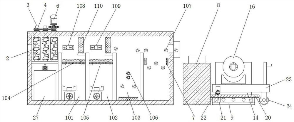
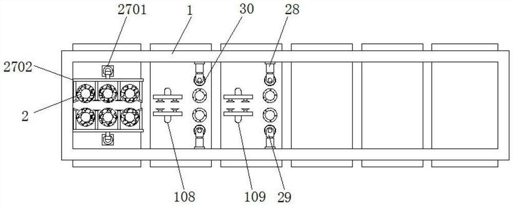
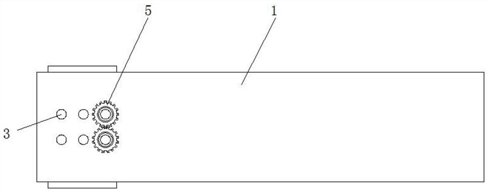
[0038] see Figure 1-7 , the present invention provides a technical solution: a cutting wire surface treatment device for semiconductor wafers, such as figure 1 , figure 2 and image 3 As shown, the inside of the device body 1 is connected with a brush roller 2 rotating close to the left side, and the upper end of the brush roller 2 penetrates the device body 1 and is connected to the first rotating shaft 3, and at the same time, the left and right first rot...


PUM


Abstract

The invention discloses a cutting steel wire surface treatment device for a semiconductor wafer. The cutting steel wire surface treatment device comprises a device body, a hot air fan, a fixing frame, a supporting plate, a collecting box and third hydraulic telescopic rods, brush rollers are rotationally connected to the position, close to the left side, in the device body, the upper ends of the brush rollers penetrate through the device body to be connected with first rotating shafts, the left first rotating shaft and the right first rotating shaft are connected through a toothed belt, the front first rotating shaft and the rear first rotating shaft on the right side are in meshed connection through first gears, the first gears are arranged on the first rotating shafts in a penetrating mode, and meanwhile the first rotating shaft on the right rear side is connected with a first motor. According to the cutting steel wire surface treatment device for the semiconductor wafer, a cutting steel wire raw material penetrates through the brush rollers, the brush rollers are driven to rotate through the gears, the toothed belt and the first rotating shaft under the action of the first motor, rust removal treatment is conducted on the cutting steel wire raw material through the brush rollers in a mechanical mode, and follow-up surface treatment machining is facilitated, and in addition, flying dust generated in the rust removal process can be sucked into the collecting box under the action of a draught fan and a suction pipe.

Description

technical field [0001] The invention relates to the technical field related to wafers, in particular to a cutting wire surface treatment device for semiconductor wafers. Background technique [0002] Wafer refers to the silicon wafer used to make silicon semiconductor circuits, and its raw material is silicon. High-purity polycrystalline silicon is dissolved and mixed with silicon crystal seeds, and then slowly pulled out to form cylindrical single crystal silicon. After the silicon ingot is ground, polished, and sliced, it forms a silicon wafer. The wafer needs to be cut into pieces during the production process. The general wafer cutting methods include laser cutting and traditional knife cutting. Saw blade or grinding wheel cutting and cutting steel wire cutting, cutting steel wire is also known as cutting steel wire, the cutting effect is second only to laser cutting, compared with laser cutting, it can effectively save energy, compared with traditional grinding wheel c...

Claims


Application Information

Patent Timeline
IPC IPC(8): B24B27/033B24B27/00B24B47/12B24B55/06B24B55/12B65H54/44B65H54/54B65H57/14B65H67/04F26B5/14
CPCB24B27/033B24B27/0076B24B47/12B24B55/06B24B55/12F26B5/14B65H54/54B65H54/44B65H57/14B65H67/0411B65H2701/30
Inventor 徐玉杰倪自飞黄河周颖楠任智伟蒋振伟张雨豪俞叔牙朱国柱
Owner NANJING VOCATIONAL UNIV OF IND TECH
Why Eureka
Try Eureka