
Method for laminating ABF layer-adding film and copper foil to inner-layer substrate

A build-up board, copper foil technology, applied in the direction of printed circuits, electrical components, printed circuit manufacturing, etc., can solve the problems of copper foil blistering, lines cannot be processed, etc.

Pending Publication Date: 2021-09-10
INST OF MICROELECTRONICS CHINESE ACAD OF SCI
View PDF3 Cites 0 Cited by
  • Summary
  • Abstract
  • Description
  • Claims
  • Application Information

AI Technical Summary

Problems solved by technology

[0006] In view of the above problems, the present invention proposes a method of pressing the ABF build-up film and copper foil to the inner substrate, in order to solve the copper foil blistering caused by the vaporization of the solvent in the ABF build-up film in the prior art, The problem that the line cannot be processed

Method used

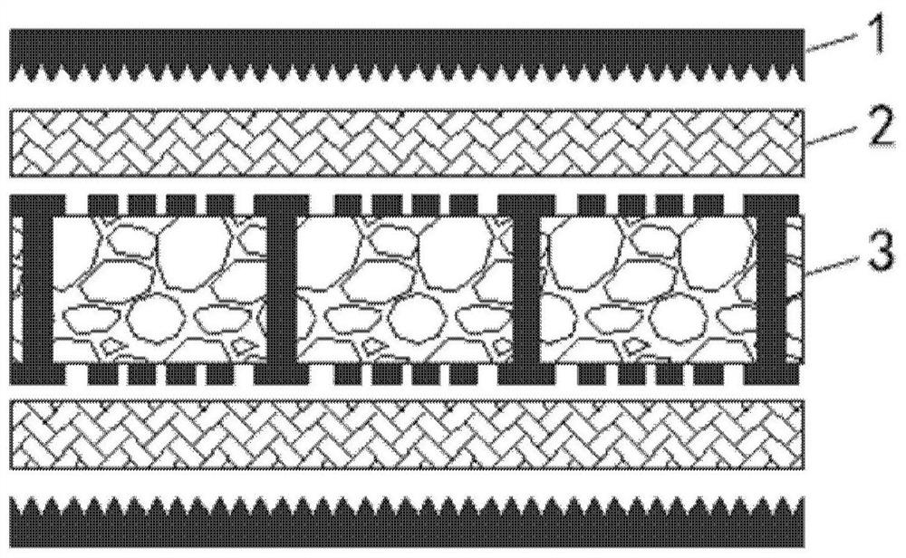
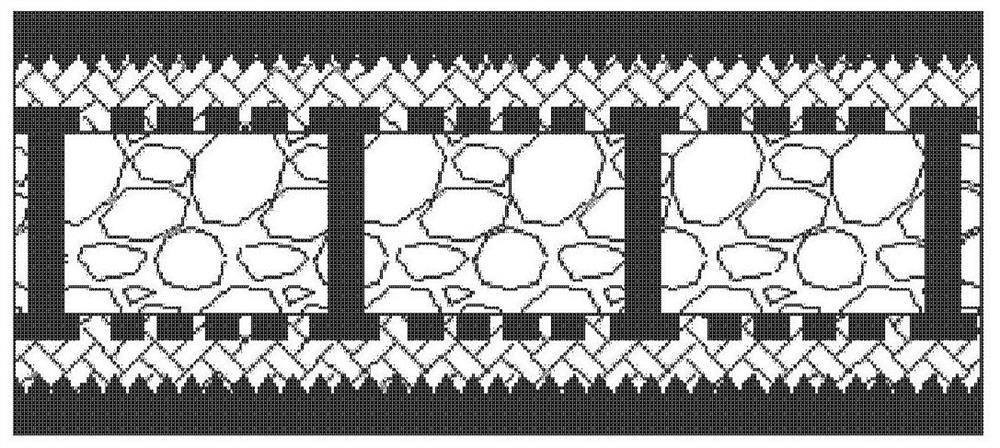

Image

  • Method for laminating ABF layer-adding film and copper foil to inner-layer substrate
  • Method for laminating ABF layer-adding film and copper foil to inner-layer substrate
  • Method for laminating ABF layer-adding film and copper foil to inner-layer substrate

Examples


Embodiment Construction

[0041] In order to make the object, technical solution and advantages of the present invention clearer, the present invention will be described in further detail below in conjunction with specific embodiments and with reference to the accompanying drawings.

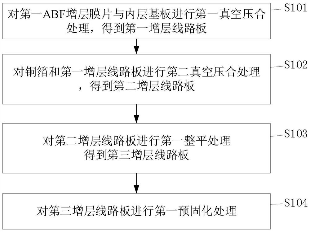
[0042] Such as figure 1 A flow chart of a method for laminating an ABF build-up film and copper foil to an inner substrate is provided for some embodiments of the present invention. In these embodiments, the implementation is as follows:

[0043] S101, keep the vacuum at the first temperature for the first vacuum time, keep the lamination state under the first pressure for the first lamination time, and perform the first vacuum lamination process on the first ABF build-up film and the inner substrate , to obtain a first build-up circuit board, wherein the first temperature is 80-130° C., preferably 100° C., the first vacuum time is 30 seconds, the first pressure is >0.5 MPa, and the first pressing time is 30 seconds.

[...


PUM


Abstract

The invention provides a method for laminating an ABF layer-adding film and a copper foil to an inner-layer substrate. The method comprises the following steps: performing first vacuum laminating treatment on a first ABF layer-adding film and the inner-layer substrate to obtain a first layer-adding circuit board; performing second vacuum lamination processing on the copper foil and the first layer-adding circuit board to obtain a second layer-adding circuit board; and performing first leveling treatment on the second layer-adding circuit board to obtain a third layer-adding circuit board. Or the method comprises: carrying out first vacuum lamination processingon the first ABF layer-adding film and the inner-layer substrate are subjected to obtain a first layer-adding circuit board; performing first vacuum lamination treatment on the second ABF layer-adding film and the copper foil to obtain a first copper foil layer-adding plate; performing second leveling treatment on the first layer-adding circuit board to obtain a fourth layer-adding circuit board; and performing first vacuum lamination processing on the fourth layer-adding circuit board and the first copper foil layer-adding board to obtain a fifth layer-adding circuit board. Or the first ABF layer-adding film and the inner-layer substrate are subjected to first vacuum lamination processing to obtain a first layer-adding circuit board; and the first layer-adding circuit board, the prepreg and the copper foil are sequentially stacked, and second vacuum lamination processing is carried out to obtain a sixth layer-adding circuit board.

Description

technical field [0001] The invention relates to the technical field of circuit board packaging, in particular to a method for laminating an ABF build-up film and copper foil to an inner substrate. Background technique [0002] Semi-additive technology is the main processing and manufacturing technology for high-density packaging substrates. For high-density packaging substrate technology, especially FCBGA packaging substrate technology, semi-additive technology has made unprecedented progress. 25um has been reduced to mass production 8um / 8um. [0003] ABF (Ajinomoto Build-up Fihn: Ajinomoto Build-up Film) material is an interlayer insulating material for high-density packaging substrate circuits produced by Ajinomoto Corporation in Japan. The ABF material does not contain glass fiber, and it is not only used in high-density wiring, but also used in other situations. For example, in the case of a thick substrate through hole with a high aspect ratio, the metallized hole nee...

Claims


Application Information

Patent Timeline
Patent Type & Authority Applications(China)
IPC IPC(8): H05K3/00
CPCH05K3/0011
Inventor 于中尧杨芳方志丹
Owner INST OF MICROELECTRONICS CHINESE ACAD OF SCI
Learn More