Dual-passband balance power division filter adopting double-layer circular patches
A filter and dual-passband technology, applied in the field of microwave passive devices, can solve the problems of large size, complex filter design, large insertion loss, etc.
- Summary
- Abstract
- Description
- Claims
- Application Information
AI Technical Summary
Problems solved by technology
Method used
Image
Examples
Embodiment 1
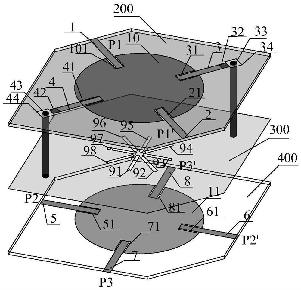
[0051] Figure 1~3 Embodiment 1 of the present invention is shown. This embodiment provides a dual-passband balanced power division filter using a double-layer circular patch, including an upper dielectric substrate 200 and a lower dielectric substrate 400. The upper dielectric substrate 200 and the lower dielectric substrate 400 are provided with a metal ground plate 300,
[0052] The upper surface of the upper dielectric substrate 200 is provided with a top-layer circular patch 10, a first input port feeder 1, a second input port feeder 2, a first isolation port 3 on the top layer, and a second isolation port 4 on the top layer. The patch 10 is located at the center of the upper dielectric substrate 200, one end of the first input port feeder 1 is connected to the edge of the upper dielectric substrate 200, and the other end is connected to the semicircle of the top circular patch 10; one end of the second input port feeder 2 It is connected to the edge of the upper layer d...
Embodiment 2
[0076] Figure 5 A modification of Embodiment 1 is shown as Embodiment 2 of the present application. Such as Figure 5 As shown, based on Embodiment 1, four rectangles are dug out from the upper dielectric substrate 200 on both sides of the first line segment AB and on both sides of the second line segment CD. The lower dielectric substrate 400 digs out two rectangles on both sides of the diagonal line EG. Two rectangles are dug out on the sides respectively, and the long sides of the rectangles lean against the edge of the metal grounding plate 300 and extend to the inside of the metal grounding plate 300; the dimensions of the above rectangles are the same.
[0077] Digging out four rectangles on the upper dielectric substrate 200 is convenient for placing four output SMA (SubMiniatureversion A) interfaces. The four output SMA interfaces are respectively connected to the first output port feeder 5, the second output port feeder 6, and the third output port feeder. 7 is co...
PUM
 Abstract
Description
Claims
Application Information
 - Generate Ideas
- Intellectual Property
- Life Sciences
- Materials
- Tech Scout
- Unparalleled Data Quality
- Higher Quality Content
- 60% Fewer Hallucinations
Browse by: Latest US Patents, China's latest patents, Technical Efficacy Thesaurus, Application Domain, Technology Topic, Popular Technical Reports.
© 2025 PatSnap. All rights reserved.Legal|Privacy policy|Modern Slavery Act Transparency Statement|Sitemap|About US| Contact US: help@patsnap.com


