High-resolution imaging device for nano material and imaging analysis method of high-resolution imaging device
An imaging device and nanomaterial technology, applied in the direction of material electrochemical variables, scattering characteristics measurement, etc., can solve the problems of reduced system detection throughput, low detection throughput, low spatial resolution, etc.
- Summary
- Abstract
- Description
- Claims
- Application Information
AI Technical Summary
Problems solved by technology
Method used
Image

Examples
Embodiment 1
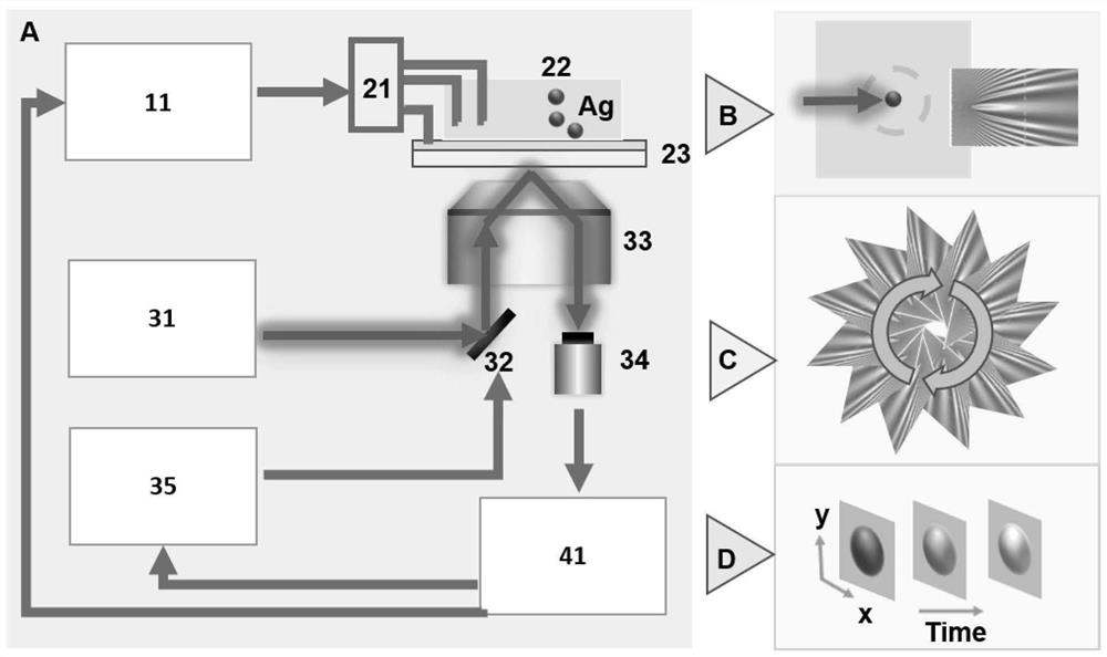
[0063] The present invention provides a high-throughput and high-resolution imaging method for nanomaterials (including zero-dimensional nanoparticles, one-dimensional nanowires, and two-dimensional nanosheet materials, etc.). The following uses Ag nanowires as an example to explore the methods used in the present invention. The devices and methods involved, and the experimental program include:
[0064] Synthesis of Ag nanowires: The Ag nanowires used in the present invention are synthesized in two steps:
[0065] 1) Synthesis of AgCl: at 800 rpm, AgNO 3 The solution (5 mL, 0.5 M) was mixed with NaCl solution (5 mL, 1M) for 1 min; the precipitate was separated from the supernatant, washed with ultrapure water and dried in vacuum;
[0066] 2) Synthesis of Ag nanowires: Dissolve 0.34 g of PVP in ethylene glycol (20 mL) and heat to 160 °C at 800 rpm; after the temperature of the solution is stable, add 25 mg of freshly prepared AgCl at one time, The solution turned bright yell...
Embodiment 2
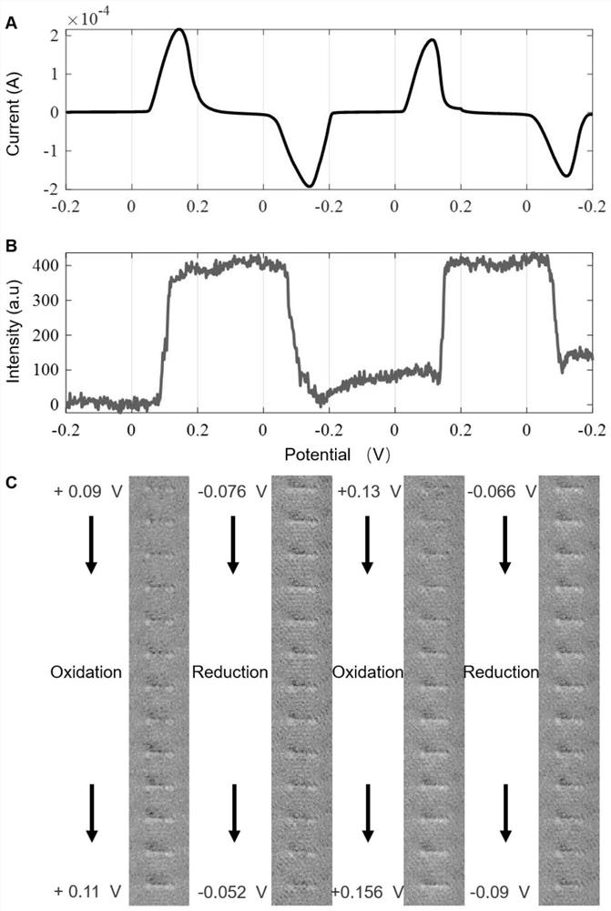
[0069] Such as image 3 , the present invention provides a method for high-resolution imaging of the electrochemical activity of a single silver (Ag) nanowire, and the steps of the determination method include:
[0070] Disperse the Ag nanowires on the Au film (23), build the electrochemical cell device, and set the parameters of the X / Y scanning galvanometer device (32) through the software control module (41);
[0071] Connect the electrochemical workstation (11), set the electrochemical test parameters, and record the optical signal and the current signal synchronously through the software control module (41).
[0072] Such as image 3 A, the oxidation peak and reduction peak begin to appear at around +0.05 V and -0.05 V (relative to Ag / AgCl reference), which is consistent with the oxidation-reduction potential of Ag under this condition reported in the literature, confirming that Ag nanowires have Electrochemical redox reactions.
[0073] Such as image 3 B, When a sin...
Embodiment 3
[0076] The present invention provides a method for high-throughput analysis and identification of different types of nanoparticles by using the difference in electrochemical activity. The following is an example of Au nanoparticles (100 nm) and Ag (100 nm) nanoparticles of the same size. Steps include:
[0077] Firstly, the Ag nanoparticles are dispersed and coated on the Au film (23 nm), the device is built, and the image is collected; the dispersed Au nanoparticles are added, and the image is collected; the two images are subtracted to determine the positions of the two particles; Connect to the electrochemical workstation (11) and set the electrochemical test parameters, and record the current signal and image signal through the software control module (41) for analysis.
[0078] Such as Figure 4 A, After completing the cyclic voltammetry (-0.2 V, +0.2 V) scan, under the same field of view, the optical signal of Au nanoparticles (green) has no obvious change, but the opti...
PUM
 Abstract
Description
Claims
Application Information
 - R&D
- Intellectual Property
- Life Sciences
- Materials
- Tech Scout
- Unparalleled Data Quality
- Higher Quality Content
- 60% Fewer Hallucinations
Browse by: Latest US Patents, China's latest patents, Technical Efficacy Thesaurus, Application Domain, Technology Topic, Popular Technical Reports.
© 2025 PatSnap. All rights reserved.Legal|Privacy policy|Modern Slavery Act Transparency Statement|Sitemap|About US| Contact US: help@patsnap.com