
Array substrate, display panel and dark spot processing method

An array substrate, dark spot technology, applied in nonlinear optics, instruments, optics, etc., can solve the problems of loss of switching function, small size, short-circuit of thin-film transistors, etc.

Pending Publication Date: 2021-08-06
HKC CORP LTD
View PDF7 Cites 1 Cited by
  • Summary
  • Abstract
  • Description
  • Claims
  • Application Information

AI Technical Summary

Problems solved by technology

[0002] Thin Film Transistor-Liquid Crystal Display (TFT-LCD) has the characteristics of small size, low power consumption, and no radiation. It has developed rapidly in recent years and occupies a dominant position in the current flat-panel display market. The actual production Due to factors such as metal residues and foreign objects, the channel of the thin film transistor may be short-circuited, causing it to lose its switching function, resulting in the pixel being displayed as a bright spot. At this time, it is usually necessary to darken the pixel. The wire is short-circuited with the pixel electrode, so that the pixel electrode has a common voltage, so that the voltage difference between the pixel electrode and the common electrode on the side of the color filter substrate is zero, and the electric field is zero, so that the liquid crystal is not deflected, the light cannot pass through, and the pixel is darkened; At present, there are some displays, in order to increase the pixel aperture ratio, the display structure of the gate storage capacitor structure is adopted, that is, the common line is not provided on the array substrate side, and the storage capacitor is formed by partially overlapping the pixel electrode and the gate line.
[0003] However, in such a storage capacitor design, the pixel electrode directly overlaps with the next row of scan lines to form a storage capacitor. Therefore, when the pixel is abnormal, it is impossible to short-circuit the pixel electrode and the common line to achieve dark spots, which seriously reduces the Product yield rate and pixel repair rate

Method used


Image

  • Array substrate, display panel and dark spot processing method
  • Array substrate, display panel and dark spot processing method
  • Array substrate, display panel and dark spot processing method

Examples


Embodiment Construction

[0033] It should be understood that the terminology and specific structural and functional details disclosed herein are representative only for describing specific embodiments, but the application can be embodied in many alternative forms and should not be construed as merely Be limited by the examples set forth herein.

[0034] In the description of the present application, the terms "first" and "second" are used for descriptive purposes only, and cannot be understood as indicating relative importance, or implicitly indicating the quantity of indicated technical features. Therefore, unless otherwise specified, the features defined as "first" and "second" may explicitly or implicitly include one or more of these features; "plurality" means two or more. The term "comprising" and any variations thereof mean non-exclusive inclusion, possible presence or addition of one or more other features, integers, steps, operations, units, components and / or combinations thereof.

[0035] Al...


PUM


Abstract

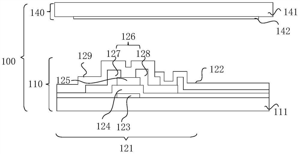
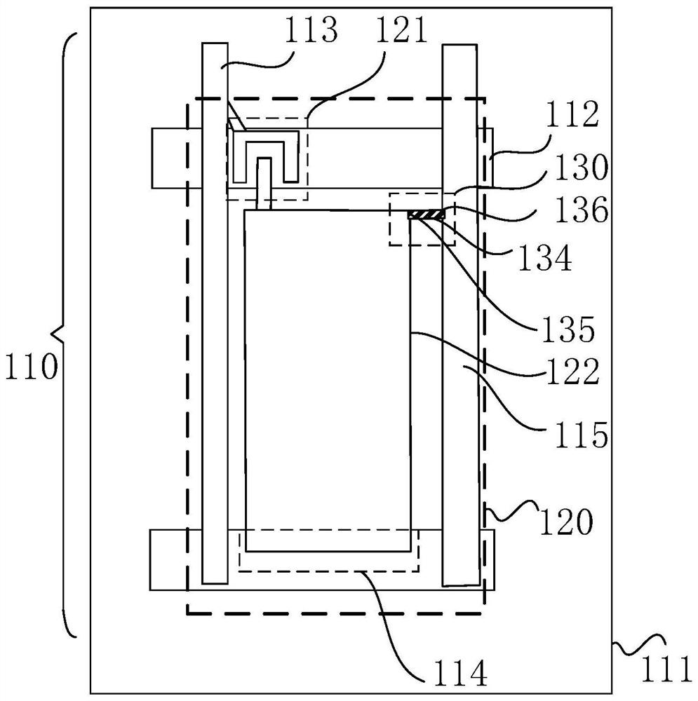
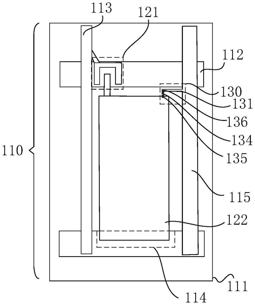
The invention discloses an array substrate, a display panel and a dark spot processing method. The array substrate comprises an array substrate body, and a plurality of scanning lines, a plurality of data lines and conductive wires which are arranged on the array substrate body, and the plurality of scanning lines and the plurality of data lines are arranged in a staggered manner to define a plurality of pixels; each pixel is provided with a pixel electrode and a thin film transistor, and the thin film transistors are respectively connected with the scanning lines, the data lines and the pixel electrodes; the pixel electrodes and the scanning lines are partially overlapped to form storage capacitors; the conductive wires are used for accessing common electrode signals, connecting parts are arranged between the conductive wires and the pixel electrodes, and the connecting parts are preset fusion points for fusing and connecting the conductive wires and the pixel electrodes; when repairing is needed, the connecting parts can be fused, the conductive wires and the pixel electrode are conducted, the potential of the pixel electrodes are pulled to the potential of the common electrode signals, and the pixel repairing rate is increased.

Description

technical field [0001] The present application relates to the field of display technology, in particular to an array substrate, a display panel and a dark spot treatment method. Background technique [0002] Thin Film Transistor-Liquid Crystal Display (TFT-LCD) has the characteristics of small size, low power consumption, and no radiation. It has developed rapidly in recent years and occupies a dominant position in the current flat-panel display market. The actual production Due to factors such as metal residues and foreign objects, the channel of the thin film transistor may be short-circuited, causing it to lose its switching function, resulting in the pixel being displayed as a bright spot. At this time, it is usually necessary to darken the pixel. The wire is short-circuited with the pixel electrode, so that the pixel electrode has a common voltage, so that the voltage difference between the pixel electrode and the common electrode on the side of the color filter substra...

Claims


Application Information

Patent Timeline
IPC IPC(8): G02F1/1362G02F1/1368
CPCG02F1/136259G02F1/1368
Inventor 宋振莉袁海江
Owner HKC CORP LTD
Learn More