Metastructure surface integrated with three-dimensional convex top layer structure
A metasurface and metasurface technology, applied in electrical components, antennas, etc., can solve the problems of difficult control of terahertz waves and harsh electromagnetic wave conditions, and achieve good isotropy, excellent insensitivity to angles, and simple structure Effect
- Summary
- Abstract
- Description
- Claims
- Application Information
AI Technical Summary
Problems solved by technology
Method used
Image
Examples
Embodiment 1
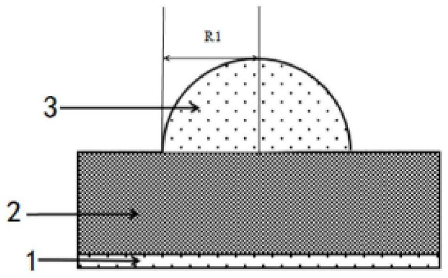
[0050] Such as figure 2 As shown, Embodiment 1 of the present invention provides a 1-bit coded metasurface whose top pattern is a solid metal hemisphere. top floor 3.
[0051] In the specific embodiment 1 of the present invention, the metasurface unit is a subwavelength array unit structure. The sub-wavelength unit structure refers to the unit structure whose structural size is at the wavelength (micron level), and has peculiar electromagnetic resonance properties, such as negative refraction, abnormal transmission, breaking through the diffraction limit, and sensitivity to dielectric environments. The resonance characteristics can be enhanced through the design of the subwavelength metal unit structure.
[0052] In the specific embodiment 1 of the present invention, the dielectric material layer 2 is made of polyimide film, and polyimide is a flexible material. As a dielectric material, the metasurface array can make the metasurface easy to bend and conform, and improve it...
Embodiment 2
[0059] A top-layer pattern provided by Embodiment 2 of the present invention is a 1-bit coded metasurface of a hollow metal hemisphere. The metasurface unit includes a metal back electrode 1, a two-dimensional dielectric material layer 2, and a three-dimensional hollow hemispherical top layer 3 arranged in sequence. Such as Figure 9 shown.
[0060] In the specific embodiment 2 of the present invention, the metasurface unit is a subwavelength array unit structure. The sub-wavelength unit structure refers to the unit structure whose structure size is much smaller than the wavelength, and has peculiar electromagnetic resonance properties, such as negative refraction, abnormal transmission, breaking through the diffraction limit, and sensitivity to dielectric environments. Resonant properties can be enhanced by subwavelength metallic structures.
[0061] In the specific embodiment 2 of the present invention, the two-dimensional dielectric material layer is made of polyimide fil...
Embodiment 3
[0068] Such as figure 2 As shown, a top-layer pattern provided by Embodiment 3 of the present invention is a 2-bit coded metasurface of a solid metal hemisphere, and the metasurface unit includes a metal back electrode 1, a two-dimensional dielectric material layer 2, and a three-dimensional solid hemisphere structure arranged in sequence top floor 3.
[0069] In the specific embodiment 3 of the present invention, the two-dimensional dielectric material layer is made of polyimide film, polyimide is a flexible material, and the metasurface array made of the dielectric material can make the metasurface bendable.
[0070] Such as figure 2 As shown, in the specific embodiment 3 of the present invention, the top layer of the three-dimensional solid hemisphere adopts metallic copper. The radii R1 of the four phase encoding unit hemispheres are 10 μm, 31.8 μm, 37.3 μm and 40 μm respectively, and the actual unit hemisphere radii may not be accurate to one or two decimal places. S...
PUM
 Abstract
Description
Claims
Application Information
 - R&D
- Intellectual Property
- Life Sciences
- Materials
- Tech Scout
- Unparalleled Data Quality
- Higher Quality Content
- 60% Fewer Hallucinations
Browse by: Latest US Patents, China's latest patents, Technical Efficacy Thesaurus, Application Domain, Technology Topic, Popular Technical Reports.
© 2025 PatSnap. All rights reserved.Legal|Privacy policy|Modern Slavery Act Transparency Statement|Sitemap|About US| Contact US: help@patsnap.com


