Flexible perovskite solar cell with high power mass ratio and preparation method thereof
A solar cell and perovskite technology, applied in circuits, photovoltaic power generation, electrical components, etc., can solve problems such as spontaneous curling of ultra-thin films, and achieve the effects of improved photoelectric conversion efficiency, low manufacturing cost, and small quality
- Summary
- Abstract
- Description
- Claims
- Application Information
AI Technical Summary
Problems solved by technology
Method used
Image
Examples
Embodiment example 1
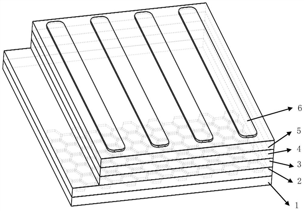
[0033] (1) Immerse the glass substrate in detergent for ultrasonic cleaning, then rinse off the detergent with deionized water, and then immerse it in deionized water, acetone and isopropanol for ultrasonic cleaning.
[0034] (2) Deposit a Parylene-C thin film on a glass substrate with a thickness of 2 μm.
[0035] (3) The surface roughness of the Parylene film is improved by using ion beam polishing technology, and the surface roughness of the film surface is controlled below 8nm.
[0036] (4) Coating a Ni metal layer on the surface of the polished Parylene-C film with a thickness of 200nm.
[0037] (5) Spin-coat photoresist on the Ni metal layer, perform photolithography after pre-baking and curing.
[0038] (6) Obtain the grid pattern formed by the photoresist by developing after photolithography.
[0039](7) Remove unnecessary metal parts by wet etching to form a conductive metal grid.
[0040] (8) Wash away the photoresist.
[0041] (9) Sputter a layer of ITO with a t...
Embodiment example 2
[0048] (1) Immerse the glass substrate in detergent for ultrasonic cleaning, then rinse off the detergent with deionized water, and then immerse it in deionized water, acetone and isopropanol for ultrasonic cleaning.
[0049] (2) Deposit a Parylene-C thin film on a glass substrate with a thickness of 2 μm.
[0050] (3) The surface roughness of the Parylene film is improved by using ion beam polishing technology, and the surface roughness of the film surface is controlled below 8nm.
[0051] (4) Coating a Ni metal layer on the surface of the polished Parylene-C film with a thickness of 200nm.
[0052] (5) Spin-coat photoresist on the Ni metal layer, perform photolithography after pre-baking and curing.
[0053] (6) Obtain the grid pattern formed by the photoresist by developing after photolithography.
[0054] (7) Remove unnecessary metal parts by wet etching to form a conductive metal grid.
[0055] (8) Wash away the photoresist.
[0056] (9) Sputter a layer of ITO with a ...
PUM
| Property | Measurement | Unit |
|---|---|---|
| thickness | aaaaa | aaaaa |
| radius | aaaaa | aaaaa |
| thickness | aaaaa | aaaaa |
Abstract
Description
Claims
Application Information
 - R&D
- Intellectual Property
- Life Sciences
- Materials
- Tech Scout
- Unparalleled Data Quality
- Higher Quality Content
- 60% Fewer Hallucinations
Browse by: Latest US Patents, China's latest patents, Technical Efficacy Thesaurus, Application Domain, Technology Topic, Popular Technical Reports.
© 2025 PatSnap. All rights reserved.Legal|Privacy policy|Modern Slavery Act Transparency Statement|Sitemap|About US| Contact US: help@patsnap.com


