Preparation method of high-quality scandium-doped aluminum nitride film template
A high-quality technology of aluminum nitride, applied in the direction of gaseous chemical plating, ion implantation plating, coating, etc., can solve the problems of low phase velocity of SAW devices, reduce the piezoelectric performance of the film, increase the acoustic loss, etc., and achieve high Acoustic phase velocity, improvement of crystallization quality, and good crystallization performance
- Summary
- Abstract
- Description
- Claims
- Application Information
AI Technical Summary
Problems solved by technology
Method used
Image
Examples
Embodiment 1
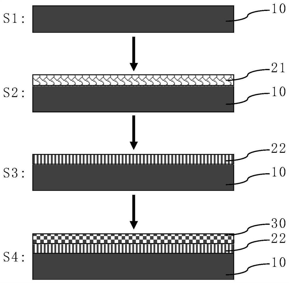
[0036] Reference attached figure 1 And attached figure 2 , in this illustrated embodiment, a method for preparing a high-quality scandium-doped aluminum nitride thin film template, including:
[0037] S1. Provide a single crystal sapphire substrate.
[0038] In this embodiment, the sapphire substrate 10 with a positive C-direction surface is provided as an example.
[0039] S2. Depositing a layer of AlN transition layer 21 on the single crystal sapphire substrate 10 by coating technology;
[0040] S3. Using high-temperature face-to-face heat treatment technology to perform high-temperature heat treatment on the AlN transition layer 21 under pure nitrogen to form a high-quality AlN buffer layer 22;
[0041] S4. Deposit scandium-doped AlN thin film 30 on AlN buffer layer 22 by DC reactive magnetron sputtering deposition method.
[0042] Steps S2 and S3 are combined with each other. Among the many coating technologies of the AlN transition layer 21, the magnetron sputtering ...
Embodiment 2
[0053] Reference attached figure 1 And attached figure 2 , in this illustrated embodiment, a method for preparing a high-quality scandium-doped aluminum nitride thin film template, including:
[0054] S1. Provide a single crystal silicon substrate. In this embodiment, the (100) crystal plane silicon substrate 40 is taken as an example.
[0055] S2. On the silicon substrate 40, first deposit a layer of SiO with a film thickness of 100 nm by using magnetron sputtering technology 2 Thin film layer 51 (process S2-1), again in SiO 2 Deposit a layer of AlN thin film layer 61 with a film thickness of 100-500 nm on the thin film layer 51 (process S2-2), and the above two layers form the transition layer 71;
[0056] S3. Using high-temperature face-to-face heat treatment technology to perform high-temperature heat treatment on the transition layer 71 under pure nitrogen to form a high-quality buffer layer 72;
[0057] S4. Depositing the scandium-doped AlN thin film 30 on the buff...
PUM
| Property | Measurement | Unit |
|---|---|---|
| thickness | aaaaa | aaaaa |
| thickness | aaaaa | aaaaa |
Abstract
Description
Claims
Application Information
 - R&D
- Intellectual Property
- Life Sciences
- Materials
- Tech Scout
- Unparalleled Data Quality
- Higher Quality Content
- 60% Fewer Hallucinations
Browse by: Latest US Patents, China's latest patents, Technical Efficacy Thesaurus, Application Domain, Technology Topic, Popular Technical Reports.
© 2025 PatSnap. All rights reserved.Legal|Privacy policy|Modern Slavery Act Transparency Statement|Sitemap|About US| Contact US: help@patsnap.com


