On-chip CMOS power amplifier with temperature compensation function

A power amplifier and temperature compensation technology, which is applied in the direction of power amplifiers, etc., can solve the problems of circuit output power gain reduction and temperature influence, and achieve precise changes in gain and output power, reduce chip area, and simplify matching circuit structure. Effect

Active Publication Date: 2021-07-23
成都知融科技有限公司
View PDF18 Cites 1 Cited by
  • Summary
  • Abstract
  • Description
  • Claims
  • Application Information

AI Technical Summary

Problems solved by technology

[0006] In view of the above-mentioned problems and defects in the prior art, the present application provides a CMOS power amplifier with a temperature compensation function on the chip, which solves the problem that the CMOS power amplifier in the prior art is greatly affected by temperature, resulting in a decrease in circuit output power and gain. question

Method used


Image

  • On-chip CMOS power amplifier with temperature compensation function
  • On-chip CMOS power amplifier with temperature compensation function
  • On-chip CMOS power amplifier with temperature compensation function

Examples


Embodiment 1

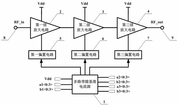
[0034] This embodiment discloses a CMOS power amplifier with temperature compensation function on chip. figure 1As shown, the power amplifier includes a multi-channel bandgap reference current source 1, a first-stage amplifying circuit 2, a second-stage amplifying circuit 3, a third-stage amplifying circuit 4, a first bias circuit 5, and a second bias circuit 6 and the third bias circuit 7, the three amplifying circuits are connected in turn, wherein the radio frequency signal input port 8 is connected to the input end of the first stage amplifying circuit 2, and the output end of the first stage amplifying circuit 2 is connected to the second stage amplifying circuit The input end of 3 is connected, the output end of the second-stage amplifying circuit 3 is connected with the input end of the third-stage amplifying circuit 4, and the output end of the third-stage amplifying circuit 4 is connected with the radio frequency signal output total port 9;

[0035] The current input...

Embodiment 2

[0040] This embodiment discloses a CMOS power amplifier with on-chip temperature compensation function. On the basis of Embodiment 1, this embodiment makes further limitations on three bias circuits and three-stage amplifying circuits.

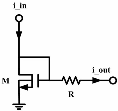
[0041] The first bias circuit 5, the second bias circuit 6 and the third bias circuit 7 have internal circuit structures such as figure 2 As shown, the circuit structures of the three are the same, including an NMOS transistor M and a resistor R, wherein the source of the NMOS transistor M is grounded, the gate and the drain are short-circuited, and the drain of the NMOS transistor M is connected to the current input terminal connected to i_in, the gate of the NMOS transistor M is connected to one end of the resistor R, and the other end of the resistor R is connected to the current output terminal i_out. The bias circuit and the NMOS tube in the amplifier form a mirror current, and the current input at the i_in terminal is mirrored to the NM...


PUM


Abstract

The invention relates to a radio frequency module integration technology applied to mobile equipment, and discloses an on-chip CMOS power amplifier with a temperature compensation function. The power amplifier comprises a multi-path band-gap reference current source, a first-stage amplifying circuit, a second-stage amplifying circuit, a third-stage amplifying circuit, a first biasing circuit, a second biasing circuit and a third biasing circuit; the multi-channel band-gap reference current source provides current for the three bias circuits, the radio frequency signal input total port is connected with the input end of the first-stage amplification circuit, the output end of the first-stage amplification circuit is connected with the input end of the second-stage amplification circuit, the output end of the second-stage amplification circuit is connected with the input end of the third-stage amplification circuit, and the output end of the third-stage amplification circuit is connected with the radio frequency signal output total port. A three-stage amplification circuit structure is adopted, gain fluctuation and output power fluctuation in high and low temperature states are compensated, and the requirements of a system can be well met.

Description

technical field [0001] This application relates to the radio frequency module integration technology applied to mobile devices, in particular to an on-chip CMOS power amplifier with temperature compensation function. Background technique [0002] With the continuous development of communication technology, wireless communication technology is becoming more and more mature. RF power amplifier is an indispensable key device in various wireless communication systems. It is mainly used to power the modulated RF signal output by the transceiver. Amplify to obtain radio frequency signals that meet the needs of wireless communication. [0003] In practical applications, it is usually required that the gain and output power of the RF power amplifier remain unchanged under high and low temperature conditions, so as to ensure that the wireless communication system can still maintain the same performance under high and low temperature environments. Refer to the attached Image 6 , due...

Claims


Application Information

Patent Timeline
Patent Type & Authority Applications(China)
IPC IPC(8): H03F3/20
CPCH03F3/20Y02D30/70
Inventor 郑中万宋柏陈涛
Owner 成都知融科技有限公司
Why Eureka
Try Eureka