Quantum dot light emitting diode and preparation method thereof
A quantum dot light-emitting and diode technology, which is used in the manufacture of semiconductor/solid-state devices, electrical components, and electric solid-state devices. Sex, the effect of avoiding agglomeration
- Summary
- Abstract
- Description
- Claims
- Application Information
AI Technical Summary
Problems solved by technology
Method used
Image
Examples
preparation example Construction
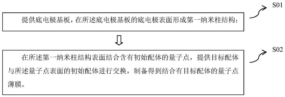
[0028] like figure 1 As shown, the first aspect of the embodiment of the present invention provides a method for preparing a quantum dot light-emitting diode, comprising the following steps:
[0029] S01. Provide a bottom electrode substrate, and form a first nanocolumn structure on the bottom electrode surface of the bottom electrode substrate;
[0030] S02. Binding quantum dots containing initial ligands on the surface of the first nanocolumn structure, providing target ligands to exchange with the initial ligands on the surface of the quantum dots, and preparing a quantum dot film bound with target ligands.
[0031] The preparation method of the quantum dot light-emitting diode provided by the embodiment of the present invention firstly forms the first nanocolumn structure on the surface of the bottom electrode of the bottom electrode substrate; Quantum dots with initial ligands enter the pores of the first nanocolumn structure, and by controlling the spacing width between...
Embodiment approach
[0064] In this embodiment, the first nanocolumn structure is not used to directly combine quantum dots and standardize the arrangement of quantum dots, but to form a second nanocolumn corresponding to the first nanocolumn structure on the surface of the first functional layer Structures provide the structural foundation. It is equivalent to forming a first functional layer with a uniform thickness on the surface of the first nano-column structure to obtain the second nano-column structure, and the gaps between the second nano-column structures are used to accommodate quantum dots. At this time, compared with the first nanocolumns, the gap between the second nanocolumns is smaller, but the maximum radial dimension of the second nanocolumns increases, specifically, the l 1 , l 2 Satisfied: l 2 1 ; At the same time, the s 1 , s 2 Meet: s 1 2 .
[0065] In order to make the quantum dots deposited in the gap between the second nanopillars have better dispersion and stability,...
Embodiment 1
[0091] like Figure 2-11 Shown, a kind of preparation method of quantum dot light-emitting diode, comprises the following steps:
[0092] Prepare ITO electrodes on transparent substrates;
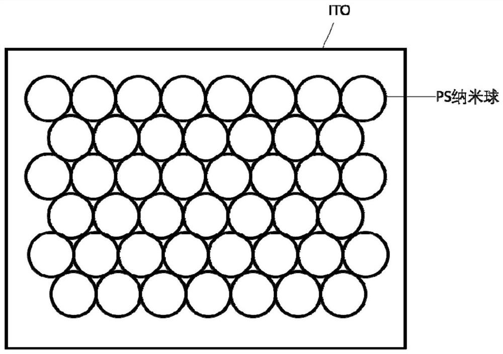
[0093] Configure a polystyrene deionized water / ethanol mixture with a polystyrene mass percentage concentration of 0.1% to 10%, and prepare a single-layer periodic ordered / disordered PS nanosphere mask on the ITO surface of the ITO electrode by self-organization method. Film, the cross-sectional view of the single-layer polystyrene nanosphere film prepared on the surface of the ITO layer is as follows figure 2 As shown, the top view of the single-layer polystyrene nanosphere film prepared on the surface of the ITO layer is as follows image 3 shown. RIE etching was performed on the prepared single-layer periodic ordered / disordered polystyrene nanosphere film to increase the gap between polystyrene nanospheres to obtain a polystyrene nanosphere mask, and polystyrene nanospheres were form...
PUM
| Property | Measurement | Unit |
|---|---|---|
| diameter | aaaaa | aaaaa |
| diameter | aaaaa | aaaaa |
| diameter | aaaaa | aaaaa |
Abstract
Description
Claims
Application Information
 - Generate Ideas
- Intellectual Property
- Life Sciences
- Materials
- Tech Scout
- Unparalleled Data Quality
- Higher Quality Content
- 60% Fewer Hallucinations
Browse by: Latest US Patents, China's latest patents, Technical Efficacy Thesaurus, Application Domain, Technology Topic, Popular Technical Reports.
© 2025 PatSnap. All rights reserved.Legal|Privacy policy|Modern Slavery Act Transparency Statement|Sitemap|About US| Contact US: help@patsnap.com


