
Epitaxial growth method, epitaxial structure and photoelectric device

A technology of epitaxial growth and epitaxial structure, which is applied in the manufacture of electrical components, semiconductor devices, semiconductor/solid-state devices, etc., can solve problems such as hindering device performance, achieve the effects of improving crystal quality, suppressing interface fluctuations, and reducing twinning

Pending Publication Date: 2021-07-09
SUZHOU INST OF NANO TECH & NANO BIONICS CHINESE ACEDEMY OF SCI
View PDF0 Cites 0 Cited by
  • Summary
  • Abstract
  • Description
  • Claims
  • Application Information

AI Technical Summary

Problems solved by technology

Autodoping can create undesired doping profiles that hinder device performance, so diffusion at the interface needs to be kept to a minimum thickness

Method used


Image

  • Epitaxial growth method, epitaxial structure and photoelectric device
  • Epitaxial growth method, epitaxial structure and photoelectric device
  • Epitaxial growth method, epitaxial structure and photoelectric device

Examples


Embodiment 1

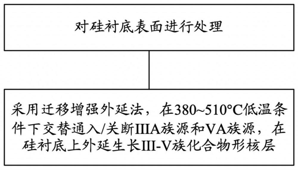
[0088] ginseng figure 2 As shown, the epitaxial growth method in this embodiment is to epitaxially grow a GaP thin film on a Si (100) substrate, which specifically includes the following steps:

[0089] 1. Treat the surface of the Si substrate.

[0090] 1.1. Clean the surface of the Si substrate.

[0091] First wash with acetone, isopropanol, and deionized water to remove organic matter on the substrate surface; then use NH 4 OH, H 2 o 2 , HCL, and deionized water for alkali cleaning and pickling; finally, HF and deionized water are used to remove surface oxides and organic matter; the cleaned Si substrate is cleaned with high-purity N 2 blow dry.

[0092] 1.2. Perform degassing pretreatment on the surface of the Si substrate.

[0093] The cleaned Si substrate is sent to the molecular beam epitaxy sample chamber for pre-degassing for 30 minutes; then sent to the pretreatment chamber for degassing at 300°C for 1.5 hours, and then sent to the growth chamber after degassin...

Embodiment 2

[0110] The epitaxial growth method in this embodiment is to epitaxially grow a GaP film on a Si(100) substrate, which specifically includes the following steps:

[0111] 1. Treat the surface of the Si substrate.

[0112] 1.1. Clean the surface of the Si substrate.

[0113] First wash with acetone, isopropanol, and deionized water to remove organic matter on the substrate surface; then use NH 4 OH, H 2 o 2 , HCL, and deionized water for alkali cleaning and pickling; finally, HF and deionized water are used to remove surface oxides and organic matter; the cleaned Si substrate is cleaned with high-purity N 2 blow dry.

[0114] 1.2. Perform degassing pretreatment on the surface of the Si substrate.

[0115] The cleaned Si substrate is sent to the molecular beam epitaxy sample chamber for pre-degassing for 30 minutes; then sent to the pretreatment chamber for degassing at 300°C for 1.5 hours, and then sent to the growth chamber after degassing is completed.

[0116] 1.3. Deoxid...


PUM


Abstract

The invention discloses an epitaxial growth method, an epitaxial structure and a photoelectric device. The method comprises the following steps: S1, processing the surface of a silicon substrate; and S2, alternately switching on / off the IIIA group source and the VA group source under the low-temperature condition of 380-510 DEG C by adopting a migration enhancement epitaxial method, and epitaxially growing the III-V group compound nucleation layer on the silicon substrate. Low-temperature growth is adopted in the initial nucleation stage, so that interface fluctuation can be effectively inhibited, a smooth and flat interface is obtained, and the crystallization quality of an epitaxial film is improved; and the anti-phase domain in the heterogeneous growth stage can be inhibited, twin crystals and stacking faults are reduced, and the dislocation density is reduced.

Description

technical field [0001] The invention belongs to the technical field of semiconductor technology, and in particular relates to an epitaxial growth method, an epitaxial structure and a photoelectric device. Background technique [0002] At present, silicon-based optoelectronic technology has made great progress and has applications in artificial intelligence, communications, high-performance computing, sensing, data centers, and autonomous driving. Silicon-based optoelectronic integration has several obvious advantages: [0003] (1) Low cost, the reserves of Si materials on the earth are very abundant, which means that the cost of raw materials is low; [0004] (2) High integration, the refractive index of Si is large, the bending radius is small, and a small device size can be achieved, so a high integration can be achieved; [0005] (3) The large-area preparation process is mature, the production process is compatible with the mature CMOS process, the production cost is lo...

Claims


Application Information

Patent Timeline
Patent Type & Authority Applications(China)
IPC IPC(8): H01L21/205H01L21/02H01L31/0304
CPCH01L21/02381H01L21/02538H01L21/02543H01L21/0262H01L31/0304H01L21/02052
Inventor 魏铁石李雪飞吴渊渊陆书龙杨文献张雪
Owner SUZHOU INST OF NANO TECH & NANO BIONICS CHINESE ACEDEMY OF SCI
Learn More