Precise circuit manufacturing method and circuit board

A manufacturing method and circuit board technology, applied in the direction of mechanical removal of conductive materials, printed circuit components, and secondary treatment of printed circuits, can solve problems such as low production efficiency, complicated procedures, and low pass rate, and achieve improved Production efficiency and qualified rate of finished products, improving signal transmission quality, and avoiding the effect of cost expenditure

Active Publication Date: 2021-07-02
SIHUI FUJI ELECTRONICS TECH
View PDF10 Cites 0 Cited by
  • Summary
  • Abstract
  • Description
  • Claims
  • Application Information

AI Technical Summary

Problems solved by technology

[0004] The wiring technology of traditional electronic circuits is mainly based on the subtractive method and semi-additive method, while both SAP (semi-additive method) and m-SAP (improved SAP method) need to use chemical copper, flash etching, electroplating, micro-etching, etc. Wet technology, the use of chemical etching method will inevitably have the problem of side erosion, the size of the side erosion is closely related to the thickness of the copper, and the thickness of the bottom copper is less than 12μm, and it will be difficult to manufacture and press the copper foil; and to increase The bonding force between the copper foil and the base material adopts the method of roughening the surface of the copper foil and the surface of the resin, which will increase the processing cost, and the roughened surface will have a bad influence on the transmission of the signal; the above process steps also have complex procedures, High energy consumption, high cost and serious environmental pollution
[0005] In addition, because the thickness of copper on the surface of the printed circuit board is generally required to be greater than 25 microns, at the same time, affected by factors such as the uniformity of electroplating copper, the development accuracy of the dry film, the alignment exposure accuracy, the uniformity of etching, and side etching, traditional printing The wire width and the spacing between wires obtained by the manufacturing method of the circuit board circuit are generally controlled above 30 μm / 30 μm (line width / spacing), and as the line width and line spacing are smaller and the density is higher, the production cost of the product is higher. The lower the pass rate, it is difficult to produce ultra-precision circuits with line width / spacing less than 30μm / 30μm, such as ultra-high-density circuits such as 20μm / 20μm, 10μm / 10μm, etc. It is difficult to manufacture more precise circuits using traditional methods However, the method of printing with high-performance conductive nano-conductive ink has the problems of difficult material preparation and extremely low production efficiency

Method used


Image

  • Precise circuit manufacturing method and circuit board

Examples


Embodiment 1

[0032] A manufacturing method of a precision circuit shown in this embodiment includes the following processing steps in sequence:

[0033] (1) Cutting: Prepare an insulating substrate with a size of 500*600 mm and a thickness of 100 μm, which is a polyimide film.

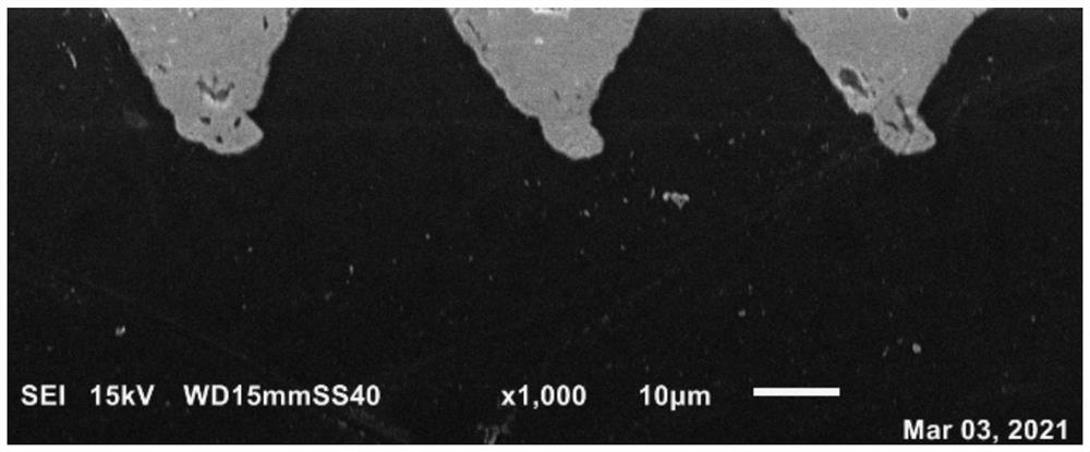
[0034] (2) Laser grooving: use a 355nm UV laser to ablate the corresponding circuit grooves on one surface of the polyimide film according to the circuit pattern required by the design; the marking speed during laser ablation is 100mm / s , the frequency is 50KHz, the pulse width is 5μS, the line width of the line groove is 20μm, the pitch (ie line gap) is 20μm, and the depth is 20μm, and the cross section of the line groove is an inverted triangle.

[0035] (3) Copper sinking: A copper layer with a thickness of 0.3 μm is deposited on the surface of the polyimide film and the inner wall of the circuit groove by chemical deposition of copper. The copper deposition layer is relatively thin. The copper layer on the sur...

Embodiment 2

[0043] The manufacturing method of a kind of precision circuit shown in this embodiment is basically the same as the manufacturing method described in Embodiment 1, the difference is that the following steps are also included after step (5):

[0044] (6) Grinding plate: After nickel sinking, the surface of the plate is smoothed by grinding the plate, so that the surface of the precision circuit is flush with the surface of the insulating substrate.

Embodiment 3

[0046] The manufacturing method of a kind of circuit board shown in the present embodiment, on the basis of the manufacturing method described in embodiment 1 or 2, namely after the nickel sinking of embodiment 1 or the grinding plate of embodiment 2, it also includes the following steps:

[0047] Subsequent process: Then make a solder resist layer on the polyimide film in sequence, immersion gold treatment for solder resist window opening, forming treatment and FQC inspection to obtain a circuit board.


PUM

PropertyMeasurementUnit
thicknessaaaaaaaaaa
thicknessaaaaaaaaaa

Abstract

The invention discloses a manufacturing method of a precise circuit and a circuit board. The manufacturing method comprises the following steps: ablating a circuit groove on the surface of an insulating substrate by using laser; depositing a copper layer on the surface of the insulating base material and the circuit groove through chemical copper deposition; removing a copper layer on the surface of the insulating base material through a grinding plate; and then depositing a nickel layer on the copper layer of the circuit groove through chemical nickel deposition, so that the circuit groove is filled and leveled up, the surface of the circuit is flattened through grinding, and the precise circuit is manufactured. According to the method, the technological process is optimized, the processes of film drying, exposure, developing, liquid medicine etching, copper plating and the like are omitted, the ultra-precise circuit with the circuit and the line distance smaller than 30 microns can be manufactured, meanwhile, the production process is optimized, and the production efficiency and the yield of finished products are improved.

Description

technical field [0001] The invention relates to the technical field of printed circuit board manufacturing, in particular to a method for manufacturing a precision circuit and a circuit board. Background technique [0002] The 21st century has entered a highly information-based society, and the demand for information consumption is becoming more and more vigorous. High-speed, high-performance, and thinner and smaller are the mainstream development trends of future electronic products. Microelectronic packaging technology is also developing at a high speed, making it lighter and lighter. There are more and more applications of devices with thinner and higher packaging density, which prompts the circuit board as a supporting platform for electronic components to change to the direction of high density, high integration and miniaturization; therefore, the wiring density of circuit boards is becoming more and more precise. The line width and spacing are gradually developing in t...

Claims


Application Information

Patent Timeline
Patent Type & Authority Applications(China)
IPC IPC(8): H05K3/04H05K3/22H05K1/11
CPCH05K3/04H05K3/22H05K1/11
Inventor 黄明安温淦尹李轩
Owner SIHUI FUJI ELECTRONICS TECH
Why Eureka
Try Eureka