Method for forming semiconductor structure and semiconductor structure

A semiconductor and patterning technology, applied in semiconductor devices, semiconductor/solid-state device manufacturing, transistors, etc., can solve the problem of increasing the aspect ratio of dielectric layers and capacitor contact holes, increasing the size of trenches, and affecting the size of capacitor contact holes, etc. question

Active Publication Date: 2022-03-01
CHANGXIN MEMORY TECH INC
View PDF8 Cites 0 Cited by
  • Summary
  • Abstract
  • Description
  • Claims
  • Application Information

AI Technical Summary

Problems solved by technology

[0002] As the line width of DRAM (Dynamic Random Access Memory, DRAM) gradually decreases, the spacing between adjacent bit line structures also gradually decreases, which will lead to the subsequent formation of dielectric between adjacent bit line structures. The aspect ratio of the layer and capacitive contact holes becomes larger
[0003] In the process of patterning the sacrificial layer and forming the trench required for the dielectric layer between adjacent bit line structures, due to the large aspect ratio of the dielectric layer, the trench formed by patterning also has a large aspect ratio, which may It will cause etching residues in the bottom sacrificial layer, and the etching residues will cause the adjacent capacitor contact holes to be connected in the subsequent process of forming capacitor contact holes, thereby affecting the yield of the semiconductor structure; if the etching residues are etched twice Etching will cause the size of the trench to become larger, thereby affecting the size of the capacitor contact hole formed later

Method used


Image

  • Method for forming semiconductor structure and semiconductor structure
  • Method for forming semiconductor structure and semiconductor structure
  • Method for forming semiconductor structure and semiconductor structure

Examples


Embodiment Construction

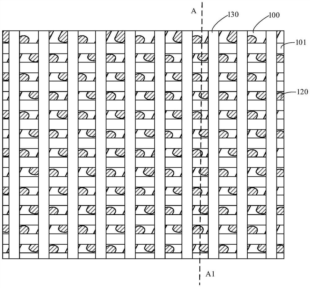
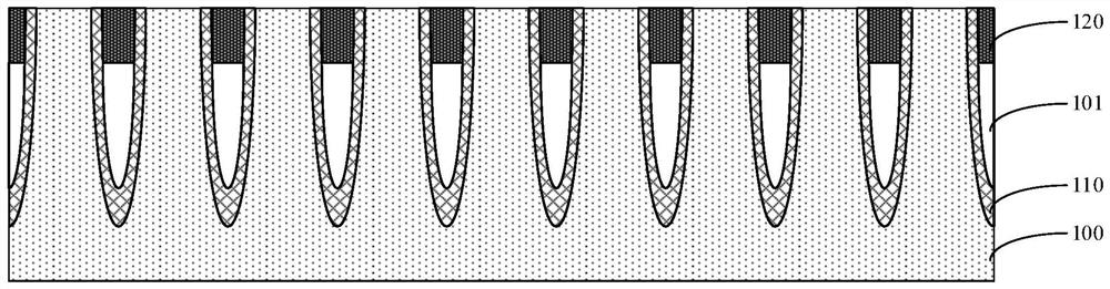
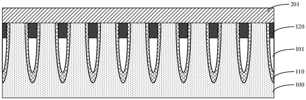
[0031] At present, the distance between adjacent bit line structures is also gradually reduced, which will lead to the increase of the aspect ratio of the dielectric layer and the capacitor contact hole formed between adjacent bit line structures; in the patterned sacrificial layer, the phase In the process of trenches required for the dielectric layer between adjacent bit line structures, due to the large aspect ratio of the dielectric layer, the trenches formed by patterning also have a large aspect ratio, which may cause etching of the bottom sacrificial layer Residue, the etching residue will cause the adjacent capacitor contact holes to be connected in the subsequent process of forming the capacitor contact hole, thus affecting the yield of the semiconductor structure; if the etching residue is etched twice, the size of the trench will be reduced becomes larger, thereby affecting the size of the capacitor contact hole formed later.

[0032] In order to solve the above pro...


PUM

PropertyMeasurementUnit
thicknessaaaaaaaaaa
thicknessaaaaaaaaaa

Abstract

Embodiments of the present application provide a method for forming a semiconductor structure and a semiconductor structure. The method for forming a semiconductor structure includes: providing a substrate on which a discrete bit line structure is formed; forming a first a sacrificial layer; forming a second sacrificial layer filling the gap of the discrete bit line structure, the second sacrificial layer is located on the top of the first sacrificial layer, and the materials of the first sacrificial layer and the second sacrificial layer are different; patterning the second sacrificial layer and The first sacrificial layer forms an opening, and in the direction in which the bit line structure extends, the formed opening and the remaining second sacrificial layer are arranged alternately; a dielectric layer filling the opening is formed; the remaining first sacrificial layer and the second sacrificial layer are removed to form a capacitor Contact holes, in the direction in which the bit line structure extends, the formed capacitive contact holes and dielectric layers are alternately arranged; the embodiment of the present application aims to form a completely etched groove without affecting the size of the dielectric layer and the capacitive contact hole groove.

Description

technical field [0001] The present application relates to the field of semiconductor forming methods, in particular to a method for forming a semiconductor structure and the semiconductor structure. Background technique [0002] As the line width of DRAM (Dynamic Random Access Memory, DRAM) gradually decreases, the spacing between adjacent bit line structures also gradually decreases, which will lead to the subsequent formation of dielectric between adjacent bit line structures. The aspect ratio of the layer and capacitive contact holes becomes larger. [0003] In the process of patterning the sacrificial layer and forming the trench required for the dielectric layer between adjacent bit line structures, due to the large aspect ratio of the dielectric layer, the trench formed by patterning also has a large aspect ratio, which may It will cause etching residues in the bottom sacrificial layer, and the etching residues will cause the adjacent capacitor contact holes to be con...

Claims


Application Information

Patent Timeline
Patent Type & Authority Patents(China)
IPC IPC(8): H01L21/8242H01L27/108
CPCH10B12/30H10B12/03H10B12/482
Inventor 洪玟基
Owner CHANGXIN MEMORY TECH INC
Why Eureka
Try Eureka