A double-heterojunction polarization-enhanced quasi-vertical gan HEMT device
A polarization-enhanced, double-heterojunction technology, used in semiconductor devices, semiconductor/solid-state device manufacturing, electrical components, etc., to solve problems such as the inability to meet the requirements of device enhancement mode operation and weaken the advantages of high-frequency operation of GaN devices , to ensure the normal realization of the function, avoid the influence of the overlay error, and improve the pressure resistance.
- Summary
- Abstract
- Description
- Claims
- Application Information
AI Technical Summary
Problems solved by technology
Method used
Image
Examples
Embodiment 1
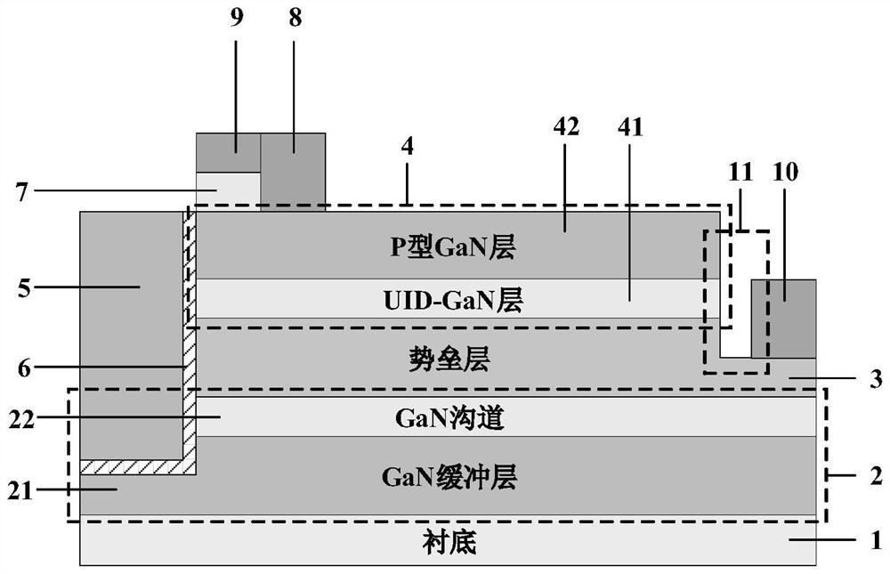
[0021] Such as figure 1 As shown, this example includes from bottom to top: a substrate 1 , a buffer layer 2 , a barrier layer 3 and a cap layer 4 . It is characterized in that: the buffer layer 2 is formed by stacking GaN buffer layer 21 and GaN channel 22 from bottom to top, and the cap layer 4 includes UID-GaN layer 41 and P-type GaN layer 42 from bottom to top ; The left end of the cap layer 4 is provided with a metal gate 5, and the metal gate 5 passes through the cap layer 4, the barrier layer 3 and the GaN trench downward from the upper surface of the cap layer 4 22, and separated from the cap layer 4, the barrier layer 3 and the buffer layer 2 by the insulating material layer 6, the lead-out end of the metal grid 5 is the gate; the upper surface of the cap layer 4 is from An N-type GaN layer 7 and a first conductive material 8 are provided from left to right, and the left side of the N-type GaN layer 7 is aligned with the interface between the insulating material laye...
Embodiment 2
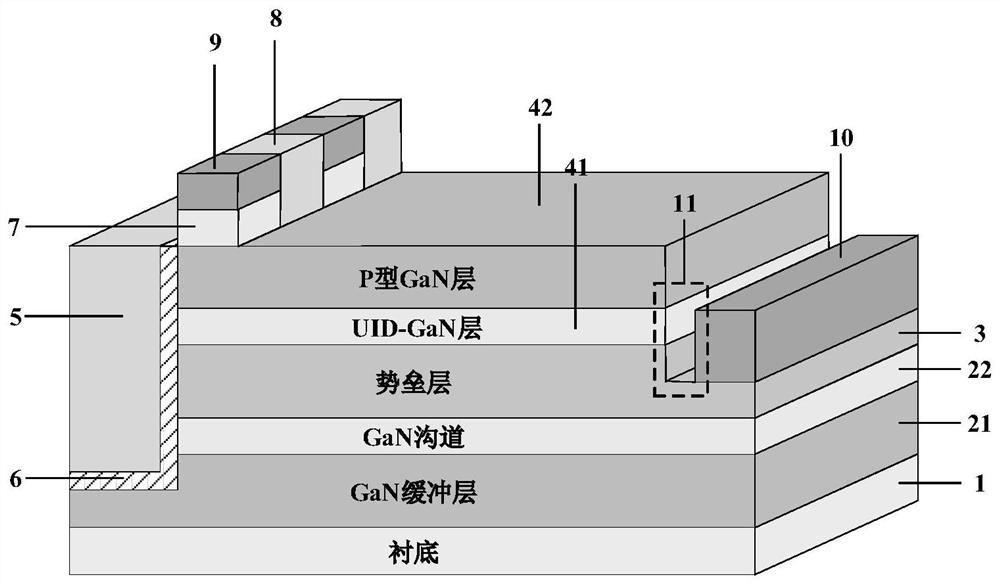
[0025] Such as figure 2 As shown, the difference between this example and the structure of Example 1 is that the stacked structure of the N-type GaN conductive region 7 and the second conductive material 9 described in this example and the first conductive material 8 are perpendicular to the device The directions of the structural sections are arranged alternately.
[0026] This example works as follows:
[0027]The electrodes are arranged alternately along the direction perpendicular to the device structure section, while saving a certain layout area, the hole current and electron flow can be adjusted by adjusting the ratio of the lengths of the two electrodes along the direction perpendicular to the device structure section. the size of the current.
Embodiment 3
[0029] This example includes a self-aligned etched gate approach for a quasi-vertical GaN HEMT device with double heterojunction polarization enhancement:
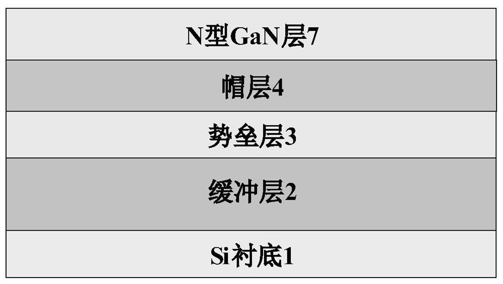
[0030] Such as image 3 As shown, using an epitaxial process, a buffer layer 2, a barrier layer 3, a cap layer 4 and an N-type GaN layer 7 are sequentially grown from bottom to top on a Si substrate 1 with a (111) crystal plane;
[0031] Such as Figure 4 As shown, a second conductive material 9 is formed on the upper surface of the N-type GaN layer 7 by using a lift-off process;
[0032] Such as Figure 5 As shown in FIG. 1 , using an etching process, a first groove is self-aligned and etched at one end of the associated N-type GaN layer 7 along the edge of the second conductive material 9, and the first groove penetrates the cap layer in sequence along the vertical direction of the device. 4. The barrier layer 3 extends into the buffer layer 2 .
PUM
 Abstract
Description
Claims
Application Information
 - Generate Ideas
- Intellectual Property
- Life Sciences
- Materials
- Tech Scout
- Unparalleled Data Quality
- Higher Quality Content
- 60% Fewer Hallucinations
Browse by: Latest US Patents, China's latest patents, Technical Efficacy Thesaurus, Application Domain, Technology Topic, Popular Technical Reports.
© 2025 PatSnap. All rights reserved.Legal|Privacy policy|Modern Slavery Act Transparency Statement|Sitemap|About US| Contact US: help@patsnap.com


